EPCS4SI8N Altera, EPCS4SI8N Datasheet - Page 23
EPCS4SI8N
Manufacturer Part Number
EPCS4SI8N
Description
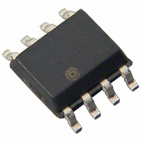
IC CONFIG DEVICE 4MBIT 8-SOIC
Manufacturer
Altera
Series
EPCSr
Datasheet
1.EPCS1SI8.pdf
(38 pages)
Specifications of EPCS4SI8N
Programmable Type
In System Programmable
Memory Size
4Mb
Voltage - Supply
3 V ~ 3.6 V
Operating Temperature
-40°C ~ 85°C
Package / Case
8-SOIC (0.154", 3.90mm Width)
Lead Free Status / RoHS Status
Lead free / RoHS Compliant
Other names
544-1379-5
EPCS4SI8N
EPCS4SI8N
Available stocks
Company
Part Number
Manufacturer
Quantity
Price
Company:

Part Number:
EPCS4SI8N
Manufacturer:
ALTERA
Quantity:
750
Part Number:
EPCS4SI8N
Manufacturer:
ALTERA/阿尔特拉
Quantity:
20 000


Chapter 3: Serial Configuration Devices (EPCS1, EPCS4, EPCS16, EPCS64, and EPCS128) Data Sheet
Serial Configuration Device Memory Access
Figure 3–14. Read Device Identification Operation Timing Diagram
Note to
(1) Only EPCS128 supports read device identification operation.
© December 2009
Figure
DCLK
ASDI
DATA
nCS
3–14:
Altera Corporation
Read Device Identification Operation
The read device identification operation code is b’1001 1111, with the MSB listed
first. Only EPCS128 supports this operation. It reads the serial configuration device’s
8-bit device identification from the DATA output pin. If this operation is shifted in
during an erase or write cycle, it is ignored and has no effect on the cycle that is in
progress.
Table 3–15. Serial Configuration Device Identification
The device implements the read device identification operation by driving nCS low
then shifting in the read device identification operation code followed by two dummy
byte on ASDI. The serial configuration device’s 16-bit device identification is then
shifted out on the DATA pin on the falling edge of DCLK, as shown in
device can terminate the read device identification operation by driving nCS high
after reading the device identification at least once.
Write Bytes Operation
The write bytes operation code is b'0000 0010, with the MSB listed first. The write
bytes operation allows bytes to be written to the memory. The write enable operation
must be executed prior to the write bytes operation to set the write enable latch bit in
the status register to 1.
The write bytes operation is implemented by driving nCS low, followed by the write
bytes operation code, three address bytes and a minimum one data byte on ASDI. If
the eight least significant address bits (A[7..0]) are not all 0, all sent data that goes
beyond the end of the current page is not written into the next page. Instead, this data
is written at the start address of the same page (from the address whose eight LSBs are
all 0). Drive nCS low during the entire write bytes operation sequence, as shown in
Figure
If more than 256 data bytes are shifted into the serial configuration device with a write
bytes operation, the previously latched data is discarded and the last 256 bytes are
written to the page. However, if less than 256 data bytes are shifted into the serial
configuration device, they are guaranteed to be written at the specified addresses and
the other bytes of the same page are unaffected.
0
High Impedance
1
2
3–15.
Operation Code
Serial Configuration Device
3
Table 3–15
4
5
EPCS128
6
shows the serial configuration device identification.
7
MSB
15
8
14
9
13
10
Two Dummy Bytes
(Note 1)
3
20
2
21
1
23
0
Configuration Handbook (Complete Two-Volume Set)
24
MSB
7
25
6
Silicon ID (Binary Value)
26
5
27
b'0001 1000
4
28
Silicon ID
3
29
2
30
1
31
Figure
0
32
3–14. The
3–23
Related parts for EPCS4SI8N
Image
Part Number
Description
Manufacturer
Datasheet
Request
R


Part Number:
Description:
IC CONFIG DEVICE 1MBIT 8-DIP
Manufacturer:
Altera
Datasheet:

Part Number:
Description:
IC CONFIG DEVICE 1.6MBIT 20-PLCC
Manufacturer:
Altera
Datasheet:
Part Number:
Description:
IC CONFIG DEVICE 1.6MBIT 20-PLCC
Manufacturer:
Altera
Datasheet:

Part Number:
Description:
IC CONFIG DEVICE 1.6MBIT 32-TQFP
Manufacturer:
Altera
Datasheet:
Part Number:
Description:
IC CONFIG DEVICE 1.6MBIT 32-TQFP
Manufacturer:
Altera
Datasheet:
Part Number:
Description:
IC CONFIG DEVICE 1.6MBIT 20-PLCC
Manufacturer:
Altera
Datasheet:
Part Number:
Description:
IC CONFIG DEVICE 1.6MBIT 20-PLCC
Manufacturer:
Altera
Datasheet:

Part Number:
Description:
IC CONFIG DEVICE 8MBIT 100-PQFP
Manufacturer:
Altera
Datasheet:
Part Number:
Description:
IC CONFIG DEVICE 1.6MBIT 32-TQFP
Manufacturer:
Altera
Datasheet:
Part Number:
Description:
IC CONFIG DEVICE 1.6MBIT 32-TQFP
Manufacturer:
Altera
Datasheet:
Part Number:
Description:
IC CONFIG DEVICE 16MBIT 100-PQFP
Manufacturer:
Altera
Datasheet:
Part Number:
Description:
IC CONFIG DEVICE 16MBIT 100-PQFP
Manufacturer:
Altera
Datasheet:
Part Number:
Description:
IC CONFIG DEVICE 16MBIT 100-PQFP
Manufacturer:
Altera
Datasheet:

Part Number:
Description:
IC CONFIG DEVICE 16MBIT 88-UBGA
Manufacturer:
Altera
Datasheet: