CY7C1020CV33-10ZXCT Cypress Semiconductor Corp, CY7C1020CV33-10ZXCT Datasheet
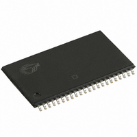
IC SRAM 512KBIT 10NS 44TSOP

CY7C1020CV33-10ZXCT

Manufacturer Part Number
CY7C1020CV33-10ZXCT
Description
IC SRAM 512KBIT 10NS 44TSOP
Manufacturer
Cypress Semiconductor Corp
Datasheet

Specifications of CY7C1020CV33-10ZXCT

Format - Memory
RAM
Memory Type
SRAM - Asynchronous
Memory Size
512K (32K x 16)
Speed
10ns
Interface
Parallel
Voltage - Supply
3 V ~ 3.6 V
Operating Temperature
0°C ~ 70°C
Package / Case
44-TSOP II
Lead Free Status / RoHS Status
Lead free / RoHS Compliant
Cypress Semiconductor Corporation
Document #: 38-05133 Rev. *E
Features
Note:
Logic Block Diagram
1. NC pins are not connected on the die
• Pin- and function-compatible with CY7C1020V33
• Temperature Ranges
• High speed
• CMOS for optimum speed/power
• Low active power
• Automatic power-down when deselected
• Independent control of upper and lower bits
• Available in Pb-free and non Pb-free 44-pin TSOP II
— Commercial: 0°C to 70°C
— Industrial: –40°C to 85°C
— Automotive: –40°C to 125°C
— t
— 325 mW (max.)
package
A
A
A
A
A
A
A
A
4
3
2
1
0
7
6
5
AA
= 10 ns
DATA IN DRIVERS
COLUMN DECODER
RAM Array
32K × 16
198 Champion Court
Functional Description
The CY7C1020CV33 is a high-performance CMOS static
RAM organized as 32,768 words by 16 bits. This device has
an automatic power-down feature that significantly reduces
power consumption when deselected.
Writing to the device is accomplished by taking Chip Enable
(CE) and Write Enable (WE) inputs LOW. If Byte Low Enable
(BLE) is LOW, then data from I/O pins (I/O
written into the location specified on the address pins (A
through A
from I/O pins (I/O
specified on the address pins (A
Reading from the device is accomplished by taking Chip
Enable (CE) and Output Enable (OE) LOW while forcing the
Write Enable (WE) HIGH. If Byte Low Enable (BLE) is LOW,
then data from the memory location specified by the address
pins will appear on I/O
LOW, then data from memory will appear on I/O
the truth table at the back of this data sheet for a complete
description of read and write modes.
The input/output pins (I/O
high-impedance state when the device is deselected (CE
HIGH), the outputs are disabled (OE HIGH), the BHE and BLE
are disabled (BHE, BLE HIGH), or during a write operation (CE
LOW, and WE LOW).
The CY7C1020CV33 is available in standard 44-pin TSOP
Type II package.
512K (32K x 16) Static RAM
I/O
I/O
14
San Jose
1
9
BHE
WE
CE
OE
BLE
). If Byte High Enable (BHE) is LOW, then data
–I/O
–I/O
8
16
9
through I/O
,
CA 95134-1709
1
Pin Configuration
to I/O
I/O
I/O
I/O
I/O
V
I/O
I/O
I/O
I/O
V
WE
A
A
A
A
NC
CE
CC
NC
A
A
A
A
SS
14
13
12
4
1
3
2
1
0
1
2
3
4
5
6
7
8
through I/O
8
1
2
3
4
5
6
7
8
9
10
11
12
13
14
15
16
17
18
19
20
21
22
. If Byte High Enable (BHE) is
16
Top View
0
TSOP II
Revised August 3, 2006
) is written into the location
through A
CY7C1020CV33
44
43
42
41
40
39
38
37
36
35
34
33
32
31
30
29
28
27
26
25
24
23
16
A
A
A
OE
BHE
BLE
I/O
I/O
I/O
I/O
V
V
I/O
I/O
I/O
I/O
NC
A
A
A
A
NC
) are placed in a
1
14
5
6
7
SS
CC
8
9
10
11
[1]
through I/O
16
15
14
13
12
11
10
9
).
9
408-943-2600
to I/O
16
. See
8
), is
0
[+] Feedback
[+] Feedback

Related parts for CY7C1020CV33-10ZXCT

CY7C1020CV33-10ZXCT Summary of contents

Page 1

... The input/output pins (I/O high-impedance state when the device is deselected (CE HIGH), the outputs are disabled (OE HIGH), the BHE and BLE are disabled (BHE, BLE HIGH), or during a write operation (CE LOW, and WE LOW). The CY7C1020CV33 is available in standard 44-pin TSOP Type II package. I/O –I/O 1 ...

Page 2

... When LOW, the I/O pins are allowed to behave as outputs. When deasserted HIGH, I/O pins are tri-stated, and act as input data pins. Ground Ground for the device. Should be connected to ground of the system. Power Supply Power Supply inputs to the device. CY7C1020CV33 -12 -15 Unit 12 15 ...

Page 3

... MHz 3.3V CC Test Conditions Test conditions follow standard test methods and procedures for measuring thermal impedance, per EIA/JESD51. CY7C1020CV33 Ambient Temperature V CC 3.3V ± 10% 0°C to +70°C 3.3V ± 10% –40°C to +85°C 3.3V ± 10% –40°C to +125°C ...

Page 4

... Document #: 38-05133 Rev. *E [4] ALL INPUT PULSES 90% 90% 10% (b) Fall Time: 1 V/ns [4] -10 Min. Max less than less than t , and t HZCE LZCE HZOE LZOE HZWE CY7C1020CV33 High-Z characteristics: R 317 Ω 3.3V 10% OUTPUT 5 pF 351Ω (c) -12 -15 Min. Max. Min. Max. Unit ...

Page 5

... CURRENT Notes: 9. Device is continuously selected. OE, CE, BHE and/or BHE = V 10 HIGH for Read cycle. 11. Address valid prior to or coincident with CE transition LOW. Document #: 38-05133 Rev OHA t RC DOE DATA VALID 50 CY7C1020CV33 DATA VALID t HZOE t HZCE t HZBE HIGH IMPEDANCE ICC CC 50% I ISB SB ...

Page 6

... Write Cycle No. 2 (BLE or BHE Controlled) ADDRESS t SA BHE, BLE WE CE DATA I/O Notes: 12. Data I/O is high impedance BHE and/or BLE = V 13 goes HIGH simultaneously with WE going HIGH, the output remains in a high-impedance state. Document #: 38-05133 Rev SCE PWE PWE t SCE CY7C1020CV33 Page [+] Feedback [+] Feedback ...

Page 7

... L H Data High High High-Z Ordering Information Speed (ns) Ordering Code 10 CY7C1020CV33-10ZC CY7C1020CV33-10ZXC 12 CY7C1020CV33-12ZC 15 CY7C1020CV33-15ZC CY7C1020CV33-15ZE CY7C1020CV33-15ZSXE Document #: 38-05133 Rev SCE PWE HZWE SD –I/O I/O –I High-Z Power-down Data Out Read—All bits High-Z Read—Lower bits only Data Out Read—Upper bits only Data In Write— ...

Page 8

... Cypress against all charges. 44-Pin TSOP II (51-85087) PIN 1 I. BASE PLANE 0°-5° 0.10 (.004) 0.597 (0.0235) 0.406 (0.0160) SEATING PLANE CY7C1020CV33 DIMENSION IN MM (INCH) MAX MIN ...

Page 9

... Document History Page Document Title: CY7C1020CV33 512K (32K x 16) Static RAM Document Number: 38-05133 REV. ECN NO. Issue Date ** 109428 12/16/01 *A 115045 05/30/02 *B 117615 08/14/02 *C 262949 See ECN *D 334398 See ECN *E 493543 See ECN Document #: 38-05133 Rev. *E Orig. of Change Description of Change HGK ...

Related keywords