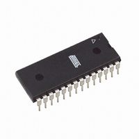
AT28C17-15PI Atmel, AT28C17-15PI Datasheet - Page 3

AT28C17-15PI
Manufacturer Part Number
AT28C17-15PI
Description
IC EEPROM 16KBIT 150NS 28DIP
Manufacturer
Atmel
Datasheet
1.AT28C17-15JC.pdf
(12 pages)
Specifications of AT28C17-15PI
Format - Memory
EEPROMs - Parallel
Memory Type
EEPROM
Memory Size
16K (2K x 8)
Speed
150ns
Interface
Parallel
Voltage - Supply
4.5 V ~ 5.5 V
Operating Temperature
-40°C ~ 85°C
Package / Case
28-DIP (0.600", 15.24mm)
Lead Free Status / RoHS Status
Contains lead / RoHS non-compliant
Other names
AT28C1715PI
Available stocks
Company
Part Number
Manufacturer
Quantity
Price
Part Number:
AT28C17-15PI
Manufacturer:
ATMEL/爱特梅尔
Quantity:
20 000
Device Operation
READ: The AT28C17 is accessed like a Static RAM.
When CE and OE are low and WE is high, the data stored
at the memory location determined by the address pins is
asserted on the outputs. The outputs are put in a high
impedance state whenever CE or OE is high. This dual line
control gives designers increased flexibility in preventing
bus contention.
BYTE WRITE: Writing data into the AT28C17 is similar to
writing into a Static RAM. A low pulse on the WE or CE
input with OE high and CE or WE low (respectively) ini-
tiates a byte write. The address location is latched on the
last falling edge of WE (or CE); the new data is latched on
the first rising edge. Internally, the device performs a self-
clear before write. Once a byte write has been started, it
will automatically time itself to completion. Once a pro-
gramming operation has been initiated and for the duration
of t
tion.
FAST BYTE WRITE: The AT28C17E offers a byte write
time of 200 s maximum. This feature allows the entire
device to be rewritten in 0.4 seconds.
READY/BUSY: Pin 1 is an open drain READY/BUSY out-
put that can be used to detect the end of a write cycle.
RDY/BUSY is actively pulled low during the write cycle and
is released at the completion of the write. The open drain
WC
, a read operation will effectively be a polling opera-
connection allows for OR-tying of several devices to the
same RDY/BUSY line.
DATA POLLING: The AT28C17 provides DATA POLLING
to signal the completion of a write cycle. During a write
cycle, an attempted read of the data being written results in
the complement of that data for I/O
indeterminate). When the write cycle is finished, true data
appears on all outputs.
WRITE PROTECTION: Inadvertent writes to the device
are protected against in the following ways: (a) V
sense—if V
inhibited; (b) V
3.8V the device will automatically time out 5 ms (typical)
before allowing a byte write; and (c) write inhibit—holding
any one of OE low, CE high or WE high inhibits byte write
cycles.
CHIP CLEAR: The contents of the entire memory of the
AT28C17 may be set to the high state by the CHIP CLEAR
operation. By setting CE low and OE to 12 volts, the chip is
cleared when a 10 msec low pulse is applied to WE.
D E V I C E I DE NT I FI C A TI O N : A n e x t r a 3 2 b y t e s o f
EEPROM memory are available to the user for device iden-
tification. By raising A9 to 12
locations 7E0H to 7FFH the additional bytes may be written
to or read from in the same manner as the regular memory
array.
CC
is below 3.8V (typical) the write function is
CC
power on delay once V
0.5V and using address
7
(the other outputs are
CC
has reached
C C
3


