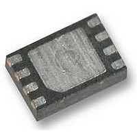
M25P20-VMP6G NUMONYX, M25P20-VMP6G Datasheet - Page 9

M25P20-VMP6G
Manufacturer Part Number
M25P20-VMP6G
Description
IC FLASH 2MBIT 50MHZ 8VFQFPN
Manufacturer
NUMONYX
Series
Forté™r
Specifications of M25P20-VMP6G
Format - Memory
FLASH
Memory Type
FLASH
Memory Size
2M (256K x 8)
Speed
50MHz
Interface
SPI, 3-Wire Serial
Voltage - Supply
2.7 V ~ 3.6 V
Operating Temperature
-40°C ~ 85°C
Package / Case
8-VFQFN, 8-VFQFPN
Clock Frequency
50MHz
Supply Voltage Range
2.7V To 3.6V
Memory Case Style
VDFPN
No. Of Pins
8
Base Number
25
Frequency
50MHz
Ic Generic Number
25P20
Memory Configuration
256K X 8
Interface Type
Serial, SPI
Rohs Compliant
Yes
Lead Free Status / RoHS Status
Lead free / RoHS Compliant
Available stocks
Company
Part Number
Manufacturer
Quantity
Price
Company:
Part Number:
M25P20-VMP6G
Manufacturer:
Micron Technology Inc
Quantity:
10 000
Part Number:
M25P20-VMP6G
Manufacturer:
ST
Quantity:
20 000
Company:
Part Number:
M25P20-VMP6GB
Manufacturer:
MICRON
Quantity:
5 600
3
Figure 3.
1. The Write Protect (W) and Hold (HOLD) signals should be driven, High or Low as appropriate.
2. These pull-up resistors, R, ensure that the memory devices are not selected if the Bus Master leaves the S line in the high-
impedance state. As the Bus Master may enter a state where all inputs/outputs are in high impedance at the same time
(e.g.: when the Bus Master is reset), the clock line (C) must be connected to an external pull-down resistor so that, when all
inputs/outputs become high impedance, S is pulled High while C is pulled Low (thus ensuring that S and C do not become
High at the same time, and so, that the t
SPI Interface with
(CPOL, CPHA) =
CS3
(0, 0) or (1, 1)
SPI Bus Master
SPI modes
These devices can be driven by a microcontroller with its SPI peripheral running in either of
the two following modes:
For these two modes, input data is latched in on the rising edge of Serial Clock (C), and
output data is available from the falling edge of Serial Clock (C).
The difference between the two modes, as shown in
bus master is in Stand-by mode and not transferring data:
Bus Master and memory devices on the SPI Bus
CS2
CPOL=0, CPHA=0
CPOL=1, CPHA=1
C remains at 0 for (CPOL=0, CPHA=0)
C remains at 1 for (CPOL=1, CPHA=1)
CS1
SDO
SDI
SCK
R
(2)
R
(2)
SHCH
C Q D
S
SPI Memory
requirement is met).
Device
W
V
CC
HOLD
R
V
(2)
SS
C Q D
S
SPI Memory
Device
Figure
W
V
HOLD
CC
R
4, is the clock polarity when the
V
(2)
SS
C Q D
S
SPI Memory
Device
W
V
CC
HOLD
AI12836
V
SS
V
V
CC
SS
9/55


