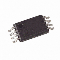
AT24C64B-10TU-1.8 Atmel, AT24C64B-10TU-1.8 Datasheet

AT24C64B-10TU-1.8
Specifications of AT24C64B-10TU-1.8
Related parts for AT24C64B-10TU-1.8
AT24C64B-10TU-1.8 Summary of contents
Page 1
... The device is optimized for use in many industrial and commercial applications where low power and low voltage operation are essential. The AT24C64B is available in space saving 8-lead JEDEC SOIC and 8-lead TSSOP packages and is accessed via a 2-wire serial interface ...
Page 2
... Device Addressing section). If the pins are left floating, the A2, A1 and A0 pins will be internally pulled down to GND if the capacitive cou- AT24C64B 2 *NOTICE: ...
Page 3
... If the pin is left floating, the WP pin will be internally pulled down to GND if the capacitive coupling to the circuit board V recommends connecting the pin to GND. 3. Memory Organization AT24C64B, 64K SERIAL EEPROM: The 64K is internally organized as 256 pages of 32 bytes each. Random word addressing requires a 13 bit data word address. Pin Capacitance (1) ...
Page 4
... This parameter is characterized and is not 100% tested (T 2. This parameter is characterized and is not 100% tested. AT24C64B 4 = -40°C to +85° Parameter (1) (2) = 25° +1.8V to +5.5V TTL Gate and CC AT24C64B 1.8V – 3.6V 5.0V Min Max Min Max 400 400 1.3 1.2 0.6 0.6 ...
Page 5
... EEPROM in 8-bit words. The EEPROM sends a zero during the ninth clock cycle to acknowl- edge that it has received each word. STANDBY MODE: The AT24C64B features a low power standby mode which is enabled: a) upon power-up and b) after the receipt of the Stop bit and the completion of any internal operations ...
Page 6
... Write Cycle Timing SCL: Serial Clock, SDA: Serial Data I/O SCL SDA 8th BIT WORDn Note: 1. The write cycle time t is the time from a valid stop condition of a write sequence to the end of the internal clear/write cycle. WR AT24C64B 6 t HIGH LOW LOW ...
Page 7
... Data Validity SDA SCL 9. Start and Stop Definition SDA SCL 10. Output Acknowledge SCL DATA IN DATA OUT 3350E–SEEPR–9/07 DATA STABLE DATA STABLE DATA CHANGE START 1 START AT24C64B STOP 8 9 ACKNOWLEDGE 7 ...
Page 8
... NOISE PROTECTION: Special internal circuitry placed on the SDA and SCL pins prevent small noise spikes from activating the device. A low-V prevent data corruption in a noisy environment. DATA SECURITY: The AT24C64B has a hardware data protection scheme that allows the user to write protect the upper quadrant (16K bits) of memory when the WP pin 12. Write Operations BYTE WRITE: A write operation requires two 8-bit data word addresses following the device address word and acknowledgment ...
Page 9
... The sequential read operation is terminated when the microcontroller does not respond with a zero but does generate a following stop condition (see Figure 13-1. Device Address 3350E–SEEPR–9/07 Figure 13-5 on page 12). Figure 13-6 AT24C64B Figure 13 page 12). 9 ...
Page 10
... Figure 13-2. Byte Write Figure 13-3. Page Write Note DON’T CARE bits Figure 13-4. Current Address Read AT24C64B 10 3350E–SEEPR–9/07 ...
Page 11
... Figure 13-5. Random Read Note DON’T CARE bits Figure 13-6. Sequential Read 3350E–SEEPR–9/07 AT24C64B 11 ...
Page 12
... AT24C64BN-10SU-2.7 (2) AT24C64BN-10SU-1.8 (2) AT24C64B-10TU-2.7 (2) AT24C64B-10TU-1.8 (3) AT24C64B-W1.8-11 Notes: 1. For 2.7V devices used in the 4.5V to 5.5V range, please refer to performance values in the AC and DC characteristics tables. 2. “U” designates Green Package & RoHS compliant. 3. Available in waffle pack and wafer form; order as SL788 for inkless wafer form. Bumped die available upon request. Please contact Serial Marketing ...
Page 13
... These drawings are for general information only. Refer to JEDEC Drawing MS-012, Variation AA for proper dimensions, tolerances, datums, etc. 1150 E. Cheyenne Mtn. Blvd. Colorado Springs, CO 80906 R 3350E–SEEPR–9/ TITLE 8S1, 8-lead (0.150" Wide Body), Plastic Gull Wing Small Outline (JEDEC SOIC) AT24C64B Ø Ø END VIEW COMMON DIMENSIONS (Unit of Measure = mm) MIN NOM MAX SYMBOL A 1.35 – 1. ...
Page 14
... Dimension b does not include Dambar protrusion. Allowable Dambar protrusion shall be 0.08 mm total in excess of the b dimension at maximum material condition. Dambar cannot be located on the lower radius of the foot. Minimum space between protrusion and adjacent lead is 0.07 mm. 5. Dimension D and determined at Datum Plane H. 2325 Orchard Parkway San Jose, CA 95131 R AT24C64B TITLE 8A2, 8-lead, 4 ...
Page 15
... Revision History Doc. Rev. 3350E 3350E–SEEPR–9/07 Date Comments 9/2007 Updated to new template; implemented revision history. AT24C64B 15 ...
Page 16
... Disclaimer: The information in this document is provided in connection with Atmel products. No license, express or implied, by estoppel or otherwise, to any intellectual property right is granted by this document or in connection with the sale of Atmel products. EXCEPT AS SET FORTH IN ATMEL’S TERMS AND CONDI- TIONS OF SALE LOCATED ON ATMEL’S WEB SITE, ATMEL ASSUMES NO LIABILITY WHATSOEVER AND DISCLAIMS ANY EXPRESS, IMPLIED OR STATUTORY WARRANTY RELATING TO ITS PRODUCTS INCLUDING, BUT NOT LIMITED TO, THE IMPLIED WARRANTY OF MERCHANTABILITY, FITNESS FOR A PARTICULAR PURPOSE, OR NON-INFRINGEMENT ...


