CY7C1069AV33-10ZXC Cypress Semiconductor Corp, CY7C1069AV33-10ZXC Datasheet
CY7C1069AV33-10ZXC
Specifications of CY7C1069AV33-10ZXC
CY7C1069AV33-10ZXC
Available stocks


Related parts for CY7C1069AV33-10ZXC

CY7C1069AV33-10ZXC Summary of contents
Page 1
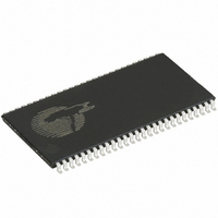
... Read and Write modes. The input/output pins (I/O impedance state when the device is deselected (CE features CE LOW), the outputs are disabled (OE HIGH), or during Write operation (CE The CY7C1069AV33 is available in a 54-pin TSOP II package with center power and ground (revolutionary) pinout. Data in Drivers ...
Page 2
... DC Electrical Characteristics .......................................... 4 Capacitance ...................................................................... 4 AC Switching Characteristics ......................................... 5 Switching Waveforms ...................................................... 7 Truth Table ........................................................................ 8 Ordering Information ........................................................ 9 Ordering Code Definition ............................................. 9 Document Number: 38-05255 Rev. *J CY7C1069AV33 Package Diagram .............................................................. 9 Acronyms ........................................................................ 10 Document Conventions ................................................. 10 Units of Measure ....................................................... 10 Document History Page ................................................. 11 Sales, Solutions, and Legal Information ...................... 12 Worldwide Sales and Design Support ....................... 12 Products .................................................................... 12 PSoC Solutions ...
Page 3
... Pin Configuration Notes 1. NC pins are not connected on the die. 2. DNU pins have to be left floating or tied ensure proper application. SS Document Number: 38-05255 Rev. *J –10 10 275 50 [1, 2] Figure 1. 54-pin TSOP II Top View I/O I I/O I DNU I/O I I/O I CY7C1069AV33 Unit Page [+] Feedback ...
Page 4
... MAX CE < 0.3 V, Max > V – 0 > V – 0 < 0 Test Conditions = 25 MHz 3 CY7C1069AV33 [3] ............................... –0 0 Ambient V CC Temperature 0 C to +70 C 3.3 V 0.3 V –40 C to +85 C –10 Unit Min Max 2.4 – V – 0 –0.3 0.8 V A – ...
Page 5
... DD time has to be provided initially before a Read/Write operation power are specified with a load capacitance ( Test Loads. Transition is measured 200 mV , and WE LOW LOW/CE HIGH 1 2 CY7C1069AV33 [5] R1 317 3.3 V OUTPUT R2 5 pF* 351 *Including jig and scope ...
Page 6
... Data setup to write end SD t Data hold from write end HIGH to low Z LZWE t WE LOW to high Z HZWE Document Number: 38-05255 Rev. *J –10 Min 7 5 – Figure 3. Data Retention Waveform DATA RETENTION MODE 3 > CDR CY7C1069AV33 Unit Max – ns – ns – ns – 3 Page [+] Feedback ...
Page 7
... Device is continuously selected 12 HIGH for Read cycle. 13. Address valid prior to or coincident with CE transition LOW and CE 1 Document Number: 38-05255 Rev. *J [11, 12] Figure 4. Read Cycle No OHA t RC DATA VALID 50 transition HIGH. 2 CY7C1069AV33 DATA VALID [12, 13] t HZOE t HZSCE HIGH IMPEDANCE 50 Page [+] Feedback ...
Page 8
... Document Number: 38-05255 Rev. *J [14, 15, 16] Controlled SCE PWE SCE PWE t t HZWE SD –I/O Mode 0 7 Power down Power down Read all bits Write all bits Selected, outputs disabled . It is active low. 2 CY7C1069AV33 [14, 15, 16 LZWE Power Standby ( Standby ( Active ( Active ( Active ( Page [+] Feedback ...
Page 9
... Ordering Information Speed (ns) Ordering Code 10 CY7C1069AV33-10ZXC Ordering Code Definition 106 9 A V33 Package Diagram Document Number: 38-05255 Rev. *J Package Package Type Diagram 51-85160 54-pin TSOP II (Pb-free) Voltage: 3.3 V Technology: 150 nm Bus Width: x8 Density: 16 Mbit Technology: CMOS Marketing Code: 7= SRAM Company Cypress Figure 8 ...
Page 10
... I/O Input/output OE Output Enable SRAM static random access memory TSOP thin small outline package TTL transistor-transistor logic WE Write Enable Document Number: 38-05255 Rev. *J CY7C1069AV33 Document Conventions Units of Measure Symbol Unit of Measure ns nano seconds V Volts µA micro Amperes mA milli Amperes mV ...
Page 11
... Document History Page Document Title: CY7C1069AV33 2 M × 8 Static RAM Document Number: 38-05255 Submission REV. ECN NO. Date ** 113724 03/27/02 *A 117060 07/31/02 *B 117990 08/30/02 *C 120385 11/13/02 *D 124441 2/25/03 *E 403984 See ECN *F 492137 See ECN *G 2784946 10/12/2009 *H 2897049 03/25/10 *I 2950666 06/11/2010 *J 3096933 11/29/2010 Document Number: 38-05255 Rev ...
Page 12
... Cypress against all charges. Use may be limited by and subject to the applicable Cypress software license agreement. Document Number: 38-05255 Rev. *J All products and company names mentioned in this document may be the trademarks of their respective holders. cypress.com/go/plc Revised November 29, 2010 CY7C1069AV33 PSoC Solutions psoc.cypress.com/solutions PSoC 1 | PSoC 3 ...