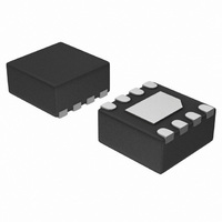
MC100LVELT23MNRG ON Semiconductor, MC100LVELT23MNRG Datasheet - Page 4

MC100LVELT23MNRG
Manufacturer Part Number
MC100LVELT23MNRG
Description
XLATOR LVPECL/LVDS-LVTTL 8-DFN
Manufacturer
ON Semiconductor
Series
100LVELTr
Datasheet
1.MC100LVELT23DTG.pdf
(8 pages)
Specifications of MC100LVELT23MNRG
Logic Function
Translator
Number Of Bits
2
Input Type
LVPECL, LVDS
Output Type
LVTTL
Number Of Channels
2
Number Of Outputs/channel
1
Differential - Input:output
Yes/No
Propagation Delay (max)
2.5ns
Voltage - Supply
3 V ~ 3.8 V
Operating Temperature
-40°C ~ 85°C
Package / Case
8-TFDFN Exposed Pad
Supply Voltage
3 V ~ 3.8 V
Lead Free Status / RoHS Status
Lead free / RoHS Compliant
Data Rate
-
Available stocks
Company
Part Number
Manufacturer
Quantity
Price
Company:
Part Number:
MC100LVELT23MNRG
Manufacturer:
ON Semiconductor
Quantity:
500
Company:
Part Number:
MC100LVELT23MNRG
Manufacturer:
ON
Quantity:
4
NOTE: Device will meet the specifications after thermal equilibrium has been established when mounted in a test socket or printed circuit
6. All values vary 1:1 with V
7. LVTTL output R
NOTE: Device will meet the specifications after thermal equilibrium has been established when mounted in a test socket or printed circuit
8. All values vary 1:1 with V
9. LVTTL output R
10. F
11. Skews are measured between outputs under identical conditions.
12. 200 mV input guarantees full logic swing at the output.
Table 5. LVTTL OUTPUT DC CHARACTERISTICS
Table 6. AC CHARACTERISTICS
V
V
I
F
t
t
t
t
t
t
V
t
t
Symbol
Symbol
OS
PLH
PHL
SK+ +
SK− −
SKPP
JITTER
r
f
max
OH
OL
PP
max
,
board with maintained transverse airflow greater than 500 lfpm. Electrical parameters are guaranteed only over the declared
operating temperature range. Functional operation of the device exceeding these conditions is not implied. Device specification limit
values are applied individually under normal operating conditions and not valid simultaneously.
guaranteed for functionality only. V
Maximum Toggle Frequency (Note 10)
Propagation Delay to
Output Differential
Output−to−Output Skew++
Output−to−Output Skew− −
Part−to−Part Skew (Note 11)
Random Clock Jitter (RMS)
Input Voltage Swing (Differential Configuration)
(Note 12)
Output Rise/Fall Times
Output HIGH Voltage (I
Output LOW Voltage (I
Output Short Circuit Current
(0.8 V − 2.0 V)
L
L
= 500 W to GND.
= 500 W to GND and C
CC
CC
Characteristic
Characteristic
. V
. V
CC
CC
Figure 2. TTL Output Loading Used for Device Evaluation
OL
*C
OH
can vary
can vary
L
= 24 mA) (Note 7)
= −3.0 mA) (Note 7)
V
includes
fixture
capacitance
CC
OL
L
= 3.3 V; GND = 0 V (Notes 8, 9)
= 20 pF to GND. Refer to Figure 2.
±
±
and V
0.3 V.
0.3 V.
OH
Q, Q
levels are guaranteed at DC only.
C
http://onsemi.com
L
V
*
CC
−180
Min
Min
180
200
330
2.4
1.0
= 3.3 V; GND = 0V (Note 6)
CHARACTERISTIC TEST
GND
APPLICATION
4
−40°C
−40°C
Typ
Typ
800
600
1.5
4.0
15
35
70
R
L
1000
TTL RECEIVER
Max
Max
−50
500
900
0.5
2.5
60
80
10
AC TEST LOAD
−180
Min
Min
180
200
330
2.4
1.0
25°C
25°C
Typ
Typ
800
600
1.7
4.0
15
40
70
1000
Max
Max
−50
500
900
0.5
2.5
70
80
10
−180
Min
Min
180
200
330
2.4
1.0
85°C
85°C
Typ
Typ
140
800
650
1.7
4.0
30
40
1000
Max
Max
−50
125
500
900
0.5
2.5
80
10
Unit
Unit
MHz
mA
mV
ns
ps
ps
ps
V
V


