NLSX3378BFCT1G ON Semiconductor, NLSX3378BFCT1G Datasheet - Page 8
NLSX3378BFCT1G
Manufacturer Part Number
NLSX3378BFCT1G
Description
XLATOR DUAL 4BIT 12-FLIPCHIP
Manufacturer
ON Semiconductor
Datasheet
1.NLSX3378FCT1G.pdf
(9 pages)
Specifications of NLSX3378BFCT1G
Logic Function
Translator, Bidirectional, Open Drain
Number Of Bits
4
Input Type
Voltage
Output Type
Voltage
Data Rate
8Mbps
Number Of Channels
4
Number Of Outputs/channel
1
Differential - Input:output
No/No
Propagation Delay (max)
30ns
Voltage - Supply
1.2 V ~ 4.1 V, 1.65 V ~ 4.5 V
Operating Temperature
-40°C ~ 85°C
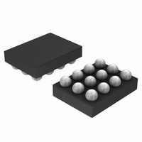
Package / Case
12-FlipChip, 12-MicroBump
Supply Voltage
1.65 V ~ 4.5 V
High Level Output Current
-20uA
Low Level Output Current
20uA
Operating Supply Voltage (min)
1.2/1.65V
Abs. Propagation Delay Time
1us
Mounting
Surface Mount
Pin Count
12
Operating Temperature (min)
-40C
Operating Temperature (max)
85C
Operating Temperature Classification
Industrial
Lead Free Status / RoHS Status
Lead free / RoHS Compliant
Available stocks
Company
Part Number
Manufacturer
Quantity
Price
Company:

Part Number:
NLSX3378BFCT1G
Manufacturer:
ON Semiconductor
Quantity:
2 200


Level Translator Architecture
bi−directional voltage level shifting to transfer data in
multiple supply voltage systems. This device has two
supply voltages, V
the input and output sides of the translator. When used to
transfer data from the V
referenced to the V
with a logic level matched to V
V
compatible to V
that independently determine the direction of the data flow
without requiring a directional pin. The one−shot circuits
are used to detect the rising or falling input signals. In
addition, the one shots decrease the rise and fall time of the
output signal for high−to−low and low−to−high transitions.
The magnitude of the pullup resistors can be reduced by
connecting external resistors in parallel to the internal
10 kW resistors.
Input Driver Requirements
drain outputs depend on the magnitude of the pull−up
resistors. In addition, the propagation times (t
(t
of the device that is connected to the translator. The timing
parameters listed in the data sheet assume that the output
impedance of the drivers connected to the translator is less
than 50 kW.
†For information on tape and reel specifications, including part orientation and tape sizes, please refer to our Tape and Reel Packaging
Specifications Brochure, BRD8011/D.
PSKEW
ORDERING INFORMATION
CC
NLSX3378FCT1G
NLSX3378BFCT1G
The
The NLSX3378 consists of two bi−directional channels
Each input/output channel has an internal 10 kW pull.
The rise (t
to V
) and maximum data rate depend on the impedance
NLSX3378 auto sense translator provides
L
translation shifts input signals with a logic level
R
) and fall (t
Device
CC
L
L
to an output signal matched to V
and V
supply are translated to output signals
L
F
CC
) timing parameters of the open
to the V
, which set the logic levels on
CC
. In a similar manner, the
CC
ports, input signals
APPLICATIONS INFORMATION
(Backside Laminate Coating)
PD
), skew
http://onsemi.com
(Pb−Free)
(Pb−Free)
mBump12
mBump12
Package
L
.
8
Enable Input (EN)
tri−state operation at the I/O pins. Driving the Enable pin
to a low logic level minimizes the power consumption of
the device and drives the I/O V
impedance state. Normal translation operation occurs
when the EN pin is equal to a logic high signal. The EN pin
is referenced to the V
Tolerant (OVT) protection.
Power Supply Guidelines
less than or equal to V
supplies will not damage the device during the power up
operation.
tri−state mode, rather than setting either the V
supplies to 0 V. The NLSX3378 will not be damaged if
either V
voltage is at a nominal operating value; however, the
operation of the translator cannot be guaranteed during
single supply operation.
capacitors should be used on the V
pins. Ceramic capacitors are a good design choice to filter
and bypass any noise signals on the voltage lines to the
ground plane of the PCB. The noise immunity will be
maximized by placing the capacitors as close as possible to
the supply and ground pins, along with minimizing the
PCB connection traces.
The NLSX3378 has an Enable pin (EN) that provides
During normal operation, supply voltage V
The enable pin should be used to enter the low current
For optimal performance, 0.01 mF to 0.1 mF decoupling
L
or V
CC
is equal to 0 V while the other supply
CC
L
3000 / Tape & Reel
3000 / Tape & Reel
. The sequencing of the power
supply and has Overvoltage
Shipping
CC
and I/O V
L
and V
†
CC
L
power supply
pins to a high
L
should be
L
or V
CC
Related parts for NLSX3378BFCT1G
Image
Part Number
Description
Manufacturer
Datasheet
Request
R

Part Number:
Description:
4-bit 20 Mb/s Dual-supply Level Translator
Manufacturer:
ON Semiconductor
Datasheet:
Part Number:
Description:
ON Semiconductor [VOLTAGE REGULATOR]
Manufacturer:
ON Semiconductor
Datasheet:
Part Number:
Description:
357-036-542-201 CARDEDGE 36POS DL .156 BLK LOPRO
Manufacturer:
ON Semiconductor
Datasheet:
Part Number:
Description:
357-036-542-201 CARDEDGE 36POS DL .156 BLK LOPRO
Manufacturer:
ON Semiconductor
Datasheet:
Part Number:
Description:
357-036-542-201 CARDEDGE 36POS DL .156 BLK LOPRO
Manufacturer:
ON Semiconductor
Datasheet:
Part Number:
Description:
357-036-542-201 CARDEDGE 36POS DL .156 BLK LOPRO
Manufacturer:
ON Semiconductor
Datasheet:
Part Number:
Description:
357-036-542-201 CARDEDGE 36POS DL .156 BLK LOPRO
Manufacturer:
ON Semiconductor
Datasheet:
Part Number:
Description:
357-036-542-201 CARDEDGE 36POS DL .156 BLK LOPRO
Manufacturer:
ON Semiconductor
Datasheet:
Part Number:
Description:
357-036-542-201 CARDEDGE 36POS DL .156 BLK LOPRO
Manufacturer:
ON Semiconductor
Datasheet:
Part Number:
Description:
357-036-542-201 CARDEDGE 36POS DL .156 BLK LOPRO
Manufacturer:
ON Semiconductor
Datasheet:
Part Number:
Description:
357-036-542-201 CARDEDGE 36POS DL .156 BLK LOPRO
Manufacturer:
ON Semiconductor
Datasheet:
Part Number:
Description:
357-036-542-201 CARDEDGE 36POS DL .156 BLK LOPRO
Manufacturer:
ON Semiconductor
Datasheet:
Part Number:
Description:
Manufacturer:
ON Semiconductor
Datasheet:
Part Number:
Description:
Manufacturer:
ON Semiconductor
Datasheet: