NLSV1T240MUTBG ON Semiconductor, NLSV1T240MUTBG Datasheet
NLSV1T240MUTBG
Specifications of NLSV1T240MUTBG
Available stocks


Related parts for NLSV1T240MUTBG

NLSV1T240MUTBG Summary of contents
Page 1
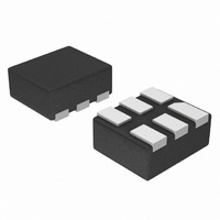
... B GND (Top View) ORDERING INFORMATION Device Package Shipping NLSV1T240MUTBG UDFN6 3000/Tape & Reel (Pb-Free) †For information on tape and reel specifications, including part orientation and tape sizes, please refer to our Tape and Reel Packaging Specification Brochure, BRD8011/D. Publication Order Number: NLSV1T240/D † ...
Page 2
PIN ASSIGNMENT PIN FUNCTION V Input Port DC Power Supply CCA V Output Port DC Power Supply CCB GND Ground A Input Port B Output Port OE Output Enable MAXIMUM RATINGS Symbol Rating Supply Voltage CCA ...
Page 3
DC ELECTRICAL CHARACTERISTICS Symbol Parameter V Input HIGH Voltage IH (A, OE) V Input LOW Voltage IL (A, OE) V Output HIGH Voltage OH V Output LOW Voltage OL I Input Leakage Current I I Power-Off Leakage Current OFF I ...
Page 4
TOTAL STATIC POWER CONSUMPTION (I 4.5 V (V) Min Max CCA 4.5 2 3.3 2 2.8 < 2 1.8 < 1 0.9 < 0.5 NOTE: Connect ground before applying supply voltage V sequence of V and V will not damage ...
Page 5
Pulse Generator Figure 2. AC (Propagation Delay) Test Circuit Test PLH PHL PLZ PZL PHZ PZH equivalent (includes probe and jig capacitance ...
Page 6
... L 5X 0.40 PITCH *For additional information on our Pb-Free strategy and soldering details, please download the ON Semiconductor Soldering and Mounting Techniques Reference Manual, SOLDERRM/D. N. American Technical Support: 800-282-9855 Toll Free USA/Canada Europe, Middle East and Africa Technical Support: Phone: 421 33 790 2910 Japan Customer Focus Center ...