NLSV4T244MUTAG ON Semiconductor, NLSV4T244MUTAG Datasheet - Page 5
NLSV4T244MUTAG
Manufacturer Part Number
NLSV4T244MUTAG
Description
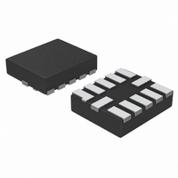
IC XLATOR 4BIT DUAL 12-UQFN
Manufacturer
ON Semiconductor
Datasheet
1.NLSV4T244MUTAG.pdf
(9 pages)
Specifications of NLSV4T244MUTAG
Logic Function
Translator, 3-State
Number Of Bits
4
Input Type
Voltage
Output Type
Voltage
Number Of Channels
4
Number Of Outputs/channel
1
Differential - Input:output
No/No
Propagation Delay (max)
1.6ns
Voltage - Supply
0.9 V ~ 4.5 V
Operating Temperature
-40°C ~ 85°C
Package / Case
12-UFQFN
Supply Voltage
3 V ~ 3.6 V
Low Level Output Current
24mA
Abs. Propagation Delay Time
5.3ns
Mounting
Surface Mount
Pin Count
12
Operating Temperature (min)
-40C
Operating Temperature (max)
85C
Operating Temperature Classification
Industrial
High Level Output Current
-24mA
Operating Supply Voltage (typ)
1.8/2.5/3.3V
Operating Supply Voltage (max)
4.5V
Operating Supply Voltage (min)
0.9V
Lead Free Status / RoHS Status
Lead free / RoHS Compliant
Data Rate
-
Lead Free Status / Rohs Status
Compliant
Available stocks
Company
Part Number
Manufacturer
Quantity
Price


NOTE: Connect ground before applying supply voltage V
1. Propagation delays defined per Figure 3.
2. Typical values are at T
3. C
TOTAL STATIC POWER CONSUMPTION (I
AC ELECTRICAL CHARACTERISTICS
CAPACITANCE
t
t
(Note 1)
t
t
(Note 1)
t
t
(Note 1)
t
t
(Note 1)
Symbol
Symbol
PLH
PHL
PZH
PZL
PHZ
PLZ
OSHL
OSLH
I
CC(operating)
C
C
C
V
PD
PD
I/O
,
CCA
,
,
IN
of V
,
4.5
3.3
2.8
1.8
0.9
is defined as the value of the IC’s equivalent capacitance from which the operating current can be calculated from:
(V)
CCA
Control Pin Input Capacitance
I/O Pin Input Capacitance
Power Dissipation Capacitance
Propagation
Delay,
A
Output
Enable,
OE to B
Output
Disable,
OE to B
Output to
Output
Skew,
Time
and V
^ C
Parameter
n
to B
PD
CCB
Min
n
n
n
x V
A
Parameter
will not damage the IC.
CC
= +25°C.
4.5
x f
IN
< 0.5
V
Max
< 2
< 1
CCA
2
2
x N
4.5
3.3
2.8
1.8
1.2
4.5
3.3
2.5
1.8
1.2
4.5
3.3
2.5
1.8
1.2
4.5
3.3
2.5
1.8
1.2
SW
(V)
where I
Min
Min
CC
3.3
4.5
CCA
V
V
V
= I
CCA
CCA
CCA
< 0.5
Max
0.15
0.15
0.15
0.15
0.15
Max
CCA
1.6
1.7
1.9
2.1
2.4
2.6
3.7
3.9
4.1
4.4
2.6
3.7
3.9
4.1
4.4
< 1
< 1
CCA
+ I
2
2
= V
= V
= V
http://onsemi.com
CCB
+ I
or V
CCB
CCB
CCB
CCB
Min
)
CCB
−405C to +855C
Min
= 3.3 V, V
= 3.3 V, V
= 3.3 V, V
and N
3.3
5
. This device is designed with the feature that the power−up sequence
V
CCB
Max
0.15
0.15
0.15
0.15
0.15
Test Conditions
2.8
1.8
1.9
2.1
2.4
2.7
3.8
3.9
4.1
4.4
4.7
3.8
3.9
4.1
4.4
4.7
SW
(V)
I
I
I
= total number of outputs switching.
< 0.5
< 0.5
Max
= 0 V or V
= 0 V or V
= 0 V or V
< 1
−405C to +855C
2
2
Min
V
CCB
2.8
CCA/B
CCA/B
CCA
(V)
Min
Max
0.15
0.15
0.15
0.15
0.15
2.0
2.1
2.3
2.5
2.8
4.0
4.1
4.3
4.5
4.8
4.0
4.1
4.3
4.5
4.8
, f = 10 MHz
1.8
Min
< 0.5
< 0.5
< 0.5
Max
2
2
1.8
Max
0.15
0.15
0.15
0.15
0.15
2.1
2.3
2.5
2.7
3.0
4.1
4.3
4.5
4.7
5.0
4.1
4.3
4.5
4.7
5.0
Min
Min
Typ (Note 2)
0.9
1.2
3.5
5.0
20
< 1.5
< 1.5
< 0.5
< 0.5
< 0.5
Max
Max
0.15
0.15
0.15
0.15
0.15
2.3
2.6
2.8
3.0
3.3
4.3
4.6
4.8
5.0
5.3
4.3
4.6
4.8
5.0
5.3
Unit
Unit
μA
μA
μA
μA
μA
nS
nS
nS
nS
Unit
pF
pF
pF
Related parts for NLSV4T244MUTAG
Image
Part Number
Description
Manufacturer
Datasheet
Request
R

Part Number:
Description:
4 Bit Unidir Translator
Manufacturer:
ON Semiconductor
Datasheet:
Part Number:
Description:
ON Semiconductor [VOLTAGE REGULATOR]
Manufacturer:
ON Semiconductor
Datasheet:
Part Number:
Description:
357-036-542-201 CARDEDGE 36POS DL .156 BLK LOPRO
Manufacturer:
ON Semiconductor
Datasheet:
Part Number:
Description:
357-036-542-201 CARDEDGE 36POS DL .156 BLK LOPRO
Manufacturer:
ON Semiconductor
Datasheet:
Part Number:
Description:
357-036-542-201 CARDEDGE 36POS DL .156 BLK LOPRO
Manufacturer:
ON Semiconductor
Datasheet:
Part Number:
Description:
357-036-542-201 CARDEDGE 36POS DL .156 BLK LOPRO
Manufacturer:
ON Semiconductor
Datasheet:
Part Number:
Description:
357-036-542-201 CARDEDGE 36POS DL .156 BLK LOPRO
Manufacturer:
ON Semiconductor
Datasheet:
Part Number:
Description:
357-036-542-201 CARDEDGE 36POS DL .156 BLK LOPRO
Manufacturer:
ON Semiconductor
Datasheet:
Part Number:
Description:
357-036-542-201 CARDEDGE 36POS DL .156 BLK LOPRO
Manufacturer:
ON Semiconductor
Datasheet:
Part Number:
Description:
357-036-542-201 CARDEDGE 36POS DL .156 BLK LOPRO
Manufacturer:
ON Semiconductor
Datasheet:
Part Number:
Description:
357-036-542-201 CARDEDGE 36POS DL .156 BLK LOPRO
Manufacturer:
ON Semiconductor
Datasheet:
Part Number:
Description:
357-036-542-201 CARDEDGE 36POS DL .156 BLK LOPRO
Manufacturer:
ON Semiconductor
Datasheet:
Part Number:
Description:
Manufacturer:
ON Semiconductor
Datasheet:
Part Number:
Description:
Manufacturer:
ON Semiconductor
Datasheet: