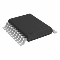
ADG3300BRUZ Analog Devices Inc, ADG3300BRUZ Datasheet - Page 17

ADG3300BRUZ
Manufacturer Part Number
ADG3300BRUZ
Description
IC XLATOR 8CH 1.2/5.5V 20TSSOP
Manufacturer
Analog Devices Inc
Datasheet
1.ADG3300BRUZ-REEL7.pdf
(20 pages)
Specifications of ADG3300BRUZ
Logic Function
Translator, Bidirectional
Number Of Bits
8
Input Type
Logic
Output Type
Logic
Data Rate
50Mbps
Number Of Channels
1
Number Of Outputs/channel
1
Differential - Input:output
No/No
Propagation Delay (max)
6ns
Voltage - Supply
1.15 V ~ 5.5 V
Operating Temperature
-40°C ~ 85°C
Package / Case
20-TSSOP
Supply Voltage
1.15 V ~ 5.5 V
No. Of Inputs
8
Propagation Delay
6ns
Logic Type
Level Translator
Supply Voltage Range
1.15V To 5.5V
Logic Case Style
TSSOP
No. Of Pins
20
Operating Temperature Range
-40°C To +85°C
High Level Output Current
-20uA
Low Level Output Current
20uA
Operating Supply Voltage (typ)
1.8/2.5/3.3/5V
Package Type
TSSOP
Operating Supply Voltage (max)
5.5V
Operating Supply Voltage (min)
1.15/1.65V
Abs. Propagation Delay Time
35ns
Mounting
Surface Mount
Pin Count
20
Operating Temperature (min)
-40C
Operating Temperature (max)
85C
Operating Temperature Classification
Industrial
Lead Free Status / RoHS Status
Lead free / RoHS Compliant
Lead Free Status / RoHS Status
Lead free / RoHS Compliant, Lead free / RoHS Compliant
Available stocks
Company
Part Number
Manufacturer
Quantity
Price
Company:
Part Number:
ADG3300BRUZ
Manufacturer:
ADI
Quantity:
1 990
Part Number:
ADG3300BRUZ
Manufacturer:
ADI/亚德诺
Quantity:
20 000
Company:
Part Number:
ADG3300BRUZ-REEL
Manufacturer:
AMS
Quantity:
3 392
APPLICATIONS
The ADG3300 is designed for digital circuits that operate at
different supply voltages; therefore, logic level translation is
required. The lower voltage logic signals are connected to the
A pins, and the higher voltage logic signals are connected to the
Y pins. The ADG3300 can provide level translation in both
directions from A Y and Y A on all eight channels, eliminating
the need for a level translator IC for each direction. The internal
architecture allows the ADG3300 to perform bidirectional level
translation without an additional signal to set the direction of
the translation. It also allows simultaneous data flow in both
directions on the same part, for example, four channels translate
in the A Y direction while the other four translate in the Y A
direction. This simplifies the design by eliminating the timing
requirements for the direction signal and reduces the number of
ICs used for level translation.
Figure 36 shows an application where a 1.8 V microprocessor
can read or write data to or from a 3.3 V peripheral device using
an 8-bit bus.
When the application requires level translation between a
microprocessor and multiple peripheral devices, the ADG3300
Y I/O pins (Y1 to Y8) can be three-stated by setting EN = 0.
This feature allows the ADG3300 to share the data buses with
MICROCONTROLLER/
MICROPROCESSOR/
DSP
1.8V
GND
Figure 36. 1.8 V to 3.3 V 8-Bit Level Translation Circuit
I/O
I/O
I/O
I/O
I/O
I/O
I/O
I/O
L
L
L
L
L
L
L
L
1
2
3
4
5
6
7
8
100nF
A1
V
A2
A3
A4
A5
A6
A7
A8
EN
CCA
ADG3300
V
GND
CCY
Y1
Y2
Y3
Y4
Y5
Y6
Y7
Y8
100nF
I/O
I/O
I/O
I/O
I/O
I/O
I/O
I/O
GND
H
H
H
H
H
H
H
H
1
2
3
4
5
6
7
8
PERIPHERAL
3.3V
DEVICE
Rev. 0 | Page 17 of 20
other devices without causing contention issues. Figure 37 shows
an application where a 3.3 V microprocessor is connected to
1.8 V peripheral devices using the three-state feature.
LAYOUT GUIDELINES
As with any high speed digital IC, the printed circuit board
layout is important in the overall circuit performance. Care
should be taken to ensure proper power supply bypass and
return paths for the high speed signals. Each V
V
(ESR) and effective series inductance (ESI) capacitors placed as
close as possible to the V
tance of the high speed signal track might cause significant
overshoot. This effect can be reduced by keeping the length
of the tracks as short as possible. A solid copper plane for the
return path (GND) is also recommended.
CCY
MICROCONTROLLER/
) should be bypassed using low effective series resistance
MICROPROCESSOR/
GND
DSP
3.3V
Figure 37. 1.8 V to 3.3 V Level Translation Circuit
CS
I/O
I/O
I/O
I/O
I/O
I/O
I/O
I/O
H
H
H
H
H
H
H
H
1
2
3
4
5
6
7
8
Using the Three-State Feature
CCA
100nF
100nF
and V
Y1
V
Y2
Y3
Y4
Y5
Y6
Y7
Y8
GND
Y1
V
Y2
Y3
Y4
Y5
Y6
Y7
Y8
GND
CCY
CCY
ADG3300
ADG3300
CCY
V
V
pins. The parasitic induc-
CCA
CCA
EN
A1
A2
A3
A4
A5
A6
A7
A8
EN
A1
A2
A3
A4
A5
A6
A7
A8
100nF
100nF
CC
I/O
I/O
I/O
I/O
I/O
I/O
I/O
I/O
GND
I/O
I/O
I/O
I/O
I/O
I/O
I/O
I/O
GND
pin (V
L
L
L
L
L
L
L
L
L
L
L
L
L
L
L
L
ADG3300
1
1
2
3
4
5
6
7
8
2
3
4
5
6
7
8
PERIPHERAL
PERIPHERAL
1.8V
1.8V
DEVICE 1
DEVICE 2
CCA
and


