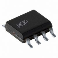
GTL2002D/DG,118 NXP Semiconductors, GTL2002D/DG,118 Datasheet - Page 4

GTL2002D/DG,118
Manufacturer Part Number
GTL2002D/DG,118
Description
IC XLATR 2BIT BI-DIREC 8-SOIC
Manufacturer
NXP Semiconductors
Datasheet
1.GTL2002DP118.pdf
(22 pages)
Specifications of GTL2002D/DG,118
Package / Case
8-SOIC (3.9mm Width)
Logic Function
Translator, Bidirectional
Number Of Bits
2
Input Type
Voltage
Output Type
Voltage
Number Of Channels
2
Number Of Outputs/channel
1
Differential - Input:output
No/No
Propagation Delay (max)
1.5ns
Voltage - Supply
3 V ~ 3.6 V
Operating Temperature
-40°C ~ 85°C
Supply Voltage
3 V ~ 3.6 V
Mounting Style
SMD/SMT
Lead Free Status / RoHS Status
Lead free / RoHS Compliant
Data Rate
-
Lead Free Status / Rohs Status
Lead free / RoHS Compliant
Other names
935287082118
GTL2002D/DG-T
GTL2002D/DG-T
GTL2002D/DG-T
GTL2002D/DG-T
NXP Semiconductors
7. Functional description
GTL2002_7
Product data sheet
6.2 Pin description
7.1 Function selection
Table 3.
Refer to
Table 4.
Assuming Dn is at the higher voltage level.
H = HIGH voltage level; L = LOW voltage level; X = Don’t care.
[1]
[2]
[3]
[4]
Table 5.
Assuming Dn is at the higher voltage level.
H = HIGH voltage level; L = LOW voltage level; X = Don’t care.
[1]
[2]
[3]
[4]
Symbol
GND
SREF
S1
S2
D2
D1
DREF
GREF
GREF
H
H
H
L
GREF
H
H
H
L
GREF should be at least 1.5 V higher than SREF for best translator operation.
Sn is not pulled up or pulled down.
Sn follows the Dn input LOW.
V
GREF should be at least 1.5 V higher than SREF for best translator operation.
Dn is pulled up to V
Dn follows the Sn input LOW.
V
TT
TT
[1]
[1]
is equal to the SREF voltage.
is equal to the SREF voltage.
Figure 1 “Functional
Pin description
Function selection, HIGH to LOW translation
Function selection, LOW to HIGH translation
Pin
SO8, TSSOP8,
XQFN8U
1
2
3
4
5
6
7
8
DREF
H
H
H
L
DREF
H
H
H
L
CC
through an external resistor.
Rev. 07 — 2 July 2009
VSSOP8
4
1
2
3
5
6
7
8
diagram”.
SREF
0 V
V
V
0 V
SREF
0 V
V
V
0 V
TT
TT
TT
TT
[4]
[4]
[4]
[4]
V
V
TT
TT
[4]
[4]
Description
ground (0 V)
source of reference transistor
port S1
port S2
port D2
port D1
drain of reference transistor
gate of reference transistor
Input Dn
X
H
L
X
Input Sn
X
V
L
X
TT
2-bit bidirectional low voltage translator
[4]
Output Sn
X
V
L
X
Output Dn
X
H
L
X
[3]
[3]
TT
[2]
[2][4]
GTL2002
© NXP B.V. 2009. All rights reserved.
Transistor
off
on
on
off
Transistor
off
nearly off
on
off
4 of 22


