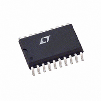
LTC1045CSW Linear Technology, LTC1045CSW Datasheet - Page 6

LTC1045CSW
Manufacturer Part Number
LTC1045CSW
Description
IC TRANSLATR/RCVR/DVR HEX 20SOIC
Manufacturer
Linear Technology
Datasheet
1.LTC1045CNPBF.pdf
(20 pages)
Specifications of LTC1045CSW
Logic Function
Programmable Translator/Receiver/Driver, 3-State
Number Of Bits
6
Input Type
TTL, CMOS
Output Type
TTL
Number Of Channels
6
Number Of Outputs/channel
1
Differential - Input:output
No/No
Propagation Delay (max)
350ns
Voltage - Supply
3 V ~ 15 V
Operating Temperature
-40°C ~ 85°C
Package / Case
20-SOIC (7.5mm Width)
Supply Voltage
3 V ~ 15 V
Lead Free Status / RoHS Status
Contains lead / RoHS non-compliant
Data Rate
-
Available stocks
Company
Part Number
Manufacturer
Quantity
Price
Company:
Part Number:
LTC1045CSW
Manufacturer:
AC
Quantity:
400
Part Number:
LTC1045CSW
Manufacturer:
LINEAR/凌特
Quantity:
20 000
Part Number:
LTC1045CSW#PBF
Manufacturer:
LINEAR/凌特
Quantity:
20 000
APPLICATIONS
The LTC1045 consists of six voltage translators and
associated control circuitry (see Block Diagram). Each
translator has a linear comparator input stage with the
positive input brought out separately. The negative inputs
of the first four comparators are tied in common to V
and the negative inputs of the last two comparators are
tied in common to V
point of the comparators can be set anywhere within the
common mode range of V
immunity each comparator has a small built-in hysteresis.
Hysteresis varies with bias current from 7mV at low bias
current to 20mV at high bias current (see typical curve of
Hysteresis vs R
Setting the Bias Current
Unlike CMOS logic, any linear CMOS circuit must draw
some quiescent current. The bias generator (Block Dia-
gram) allows the quiescent current of the comparators to
be varied. Bias current is programmed with an external
resistor (see typical curve of I
current is decreased, the LTC1045 slows down (see
typical curve of Delay Time vs R
Shutting Power Off and Latching the Outputs
In addition to setting the bias current, the I
power completely off and latches the translator outputs.
To do this, the I
shown in Figure 4, a CMOS gate or a TTL gate with a
resistor pull-up does this quite nicely. Even though power
LTC1045
6
10
(A) CMOS
LTC1045
Figure 4. Driving the I
12
20
SET
SET
4.5V TO 15V
).
U
TRIP2
pin must be forced to V
V+
. With these inputs the switching
INFORMATION
U
–
to V
10
SET
+
+
SET
Pin with Logic
– 2V. To improve noise
LTC1045
vs R
(B) TTL
W
).
SET
). As the bias
20
12
SET
+
4.5V TO 5.5V
– 0.5V. As
U
pin shuts
V+
100k
TRIP1
1045 F04
is turned off to the linear circuitry, the CMOS output logic
is powered and maintains the output state. With no DC
load on the output, power dissipation, for all practical
purposes, is zero.
Latching the output is fast—typically 80ns from the rising
edge of I
is much slower—typically 1.5 s from the falling edge of
I
During the power-up time, the output can assume false
states. To avoid problems, the output should not be
considered valid until 2 s to 5 s after the falling edge of
I
Putting the Outputs in Hi-Z State
A DISABLE input sets the six outputs to a high impedance
state. This allows the LTC1045 to be interfaced to a data
bus. When DISABLE = “1” the outputs are high impedance
and when DISABLE = “0” they are active. With TTL
supplies, V
input is TTL compatible.
Power Supplies
There are four power supplies on the LTC1045: V
V
there are a few restrictions. A minimum differential must
exist between V
differential must be at least 4.5V and the V
differential must be at least 3V. Another restriction is
caused by the internal parasitic diode D1 (see Figure 5).
SET
SET
OH
. This time is set by the comparator’s power-up time.
.
and V
DISABLE
DISABLE
SET
DATA
OL
+
. Going from the latched to flow-through state
. They can be connected almost arbitrarily, but
= 4.5V to 5.5V and V
+
and V
Figure 5. Output Driver
V
V
V
V
OL
OL
+
+
–
and V
V
V
OH
OL
OH
P1
N1
D1
–
and V
= GND, the DISABLE
V
+
OL
. The V
OUTPUT
PIN
OH
1045 F05
+
to V
+
to V
, V
1045fc
OL
–
–
,


