NLSX4014MUTAG ON Semiconductor, NLSX4014MUTAG Datasheet
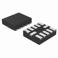
IC LVL XLATOR 4-BIT DUAL 12UQFN

NLSX4014MUTAG

Manufacturer Part Number
NLSX4014MUTAG
Description
IC LVL XLATOR 4-BIT DUAL 12UQFN
Manufacturer
ON Semiconductor
Datasheet

Specifications of NLSX4014MUTAG

Logic Function
Translator, Bidirectional
Number Of Bits
4
Input Type
Voltage
Output Type
Voltage
Data Rate
140Mbps
Number Of Channels
4
Number Of Outputs/channel
1
Differential - Input:output
No/No
Propagation Delay (max)
6.5ns
Voltage - Supply
0.9 V ~ 4.1 V, 1.3 V ~ 4.5 V
Operating Temperature
-40°C ~ 85°C
Package / Case
12-UFQFN
Supply Voltage
1.3 V ~ 4.5 V
Lead Free Status / RoHS Status
Lead free / RoHS Compliant
Other names
NLSX4014MUTAGOSTR

Available stocks

Company
Part Number
Manufacturer
Quantity
Price
Part Number:
NLSX4014MUTAG
Manufacturer:
ON Semiconductor
Quantity:
500
Company:
Part Number:
NLSX4014MUTAG
Quantity:
3 000
NLSX4014
4-Bit 100 Mb/s Configurable
Dual-Supply Level
Translator
level translator without a direction control pin. The I/O V
V
and V
to 4.5 V while the V
− 0.4) V. This allows lower voltage logic signals on the V
translated into higher voltage logic signals on the V
vice−versa. Both I/O ports are auto−sensing; thus, no direction pin is
required.
by putting them in 3−state. This significantly reduces the supply
currents from both V
V
Features
Typical Applications
© Semiconductor Components Industries, LLC, 2009
December, 2009 − Rev. 3
L
L
The NLSX4014 is a 4−bit configurable dual−supply bidirectional
The Output Enable (EN) input, when Low, disables both I/O ports
Wide Low−Side V
Wide High−Side V
Power Supply Isolation
High−Speed with 100 Mb/s Guaranteed Date Rate for V
Low Bit−to−Bit Skew
Overvoltage Tolerant Enable and I/O Pins
Non−preferential Powerup Sequencing
Small packaging: 1.7 mm x 2.0 mm UQFN12
These are Pb−Free Devices
Mobile Phones, PDAs, Other Portable Devices
−ports are designed to track two different power supply rails, V
.
is at Ground
All Outputs are in the High Impedance State if Either V
L
respectively. The V
L
CC
L
CC
supply rail is configurable from 0.9 V to (V
Operating Range: 0.9 V to (V
and V
Operating Range: 1.3 V to 4.5 V
CC
supply rail is configurable from 1.3 V
L
. The EN signal is designed to track
CC
CC
− 0.4) V
CC
L
side to be
L
side, and
− and I/O
1
> 1.6 V
L
or V
CC
CC
CC
14
†For information on tape and reel specifications,
NLSX4014MUTAG
NLSX4014DR2G
NLSX4014DTR2G
14
including part orientation and tape sizes, please
refer to our Tape and Reel Packaging Specification
Brochure, BRD8011/D.
1
(Note: Microdot may be in either location)
1
A
L, WL
Y, YY
W, WW
G or G
(Note: Microdot may be in either location)
Device
1
ORDERING INFORMATION
WA = Specific Device Code
M
G
CASE 523AE
http://onsemi.com
CASE 751A
MU SUFFIX
= Assembly Location
= Wafer Lot
= Year
= Work Week
= Pb−Free Package
= Date Code
= Pb−Free Package
D SUFFIX
CASE 948G
DT SUFFIX
SOIC−14
TSSOP−14
UQFN12
(Pb−Free)
(Pb−Free)
TSSOP14
(Pb−Free)
Package
UQFN12
SO−14
Publication Order Number:
14
1
3000/T ape & Reel
2500/T ape & Reel
2500/T ape & Reel
DIAGRAMS
14
NLSX4014G
MARKING
AWLYWW
1
Shipping
WAMG
NLSX4014/D
ALYWG
NLSX
G
4014
G

Related parts for NLSX4014MUTAG

NLSX4014MUTAG Summary of contents

Page 1

... Year Work Week Pb−Free Package (Note: Microdot may be in either location) ORDERING INFORMATION Device NLSX4014MUTAG NLSX4014DR2G NLSX4014DTR2G †For information on tape and reel specifications, including part orientation and tape sizes, please refer to our Tape and Reel Packaging Specification Brochure, BRD8011/D. 1 MARKING DIAGRAMS ...

Page 2

GND (Top View) I/O V I/O V I/O V ...

Page 3

NLSX4014 +1.8 V System I I I/ GND EN EN GND Figure 3. Typical Application Circuit V L +3.6V CC +3.6 V System ...

Page 4

MAXIMUM RATINGS Symbol Parameter V V Supply Voltage Supply Voltage −Referenced DC Input/Output Voltage −Referenced DC Input/Output Voltage Enable Control Pin DC Input ...

Page 5

DC ELECTRICAL CHARACTERISTICS Symbol Parameter V I/O V Input HIGH IHC CC Voltage V I/O V Input LOW ILC CC Voltage V I/O V Input HIGH IHL L Voltage V I/O V Input LOW ILL L Voltage V Control Pin ...

Page 6

POWER CONSUMPTION Symbol Parameter I Supply Current from Q−VCC V I CCn I Supply Current from Q− CCn I/O V CCn I V Tristate ...

Page 7

TIMING CHARACTERISTICS Symbol Parameter t I/O V Rise Time R−VCC CC (Output = I/O_V ) CC t I/O V Falltime F−VCC CC (Output = I/O_V ) CC t I/O V Risetime R−VL L (Output = I/O_V ) L t I/O ...

Page 8

ENABLE / DISABLE TIME MEASUREMENTS Symbol Parameter t Turn−On Enable Time (Output = EN−VCC I/O_V , pZH Turn−On Enable Time (Output = I/O_V , pZL t Turn−On Enable Time (Output = EN−VL I/O_V , ...

Page 9

PULSE GENERATOR PZH PHZ PZL PLZ equivalent (Includes jig and probe capacitance OUT Figure 7. Test Circuit for Enable/Disable ...

Page 10

IMPORTANT APPLICATIONS INFORMATION Level Translator Architecture The NLSX4014 auto sense translator provides bi−directional voltage level shifting to transfer data in multiple supply voltage systems. This device has two supply voltages, V and V , which set the logic levels on ...

Page 11

... M NOTE 3 0.32 2.30 11X 0.22 *For additional information on our Pb−Free strategy and soldering details, please download the ON Semiconductor Soldering and Mounting Techniques Reference Manual, SOLDERRM/D. http://onsemi.com 11 NOTES: 1. DIMENSIONING AND TOLERANCING PER ASME Y14.5M, 1994. 2. CONTROLLING DIMENSION: MILLIMETERS 3. DIMENSION b APPLIES TO PLATED TERMINAL AND IS MEASURED BETWEEN 0 ...

Page 12

G −T− SEATING 14 PL PLANE 0.25 (0.010 PACKAGE DIMENSIONS SOIC−14 D SUFFIX CASE 751A−03 ISSUE 0.25 (0.010 ...

Page 13

... SCILLC is an Equal Opportunity/Affirmative Action Employer. This literature is subject to all applicable copyright laws and is not for resale in any manner. PUBLICATION ORDERING INFORMATION LITERATURE FULFILLMENT: Literature Distribution Center for ON Semiconductor P.O. Box 5163, Denver, Colorado 80217 USA Phone: 303−675−2175 or 800−344−3860 Toll Free USA/Canada Fax: 303− ...

Related keywords