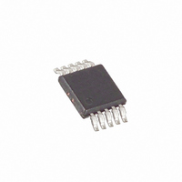
MAX9376EUB+ Maxim Integrated Products, MAX9376EUB+ Datasheet - Page 3

MAX9376EUB+
Manufacturer Part Number
MAX9376EUB+
Description
IC TRANSLATOR DUAL 10-UMAX
Manufacturer
Maxim Integrated Products
Datasheet
1.MAX9376EUB.pdf
(8 pages)
Specifications of MAX9376EUB+
Logic Function
Translator
Number Of Bits
2
Input Type
AnyLevel™
Output Type
LVDS, LVPECL
Number Of Channels
2
Number Of Outputs/channel
2
Differential - Input:output
Yes/No
Voltage - Supply
3 V ~ 3.6 V
Operating Temperature
-40°C ~ 85°C
Package / Case
10-MSOP, Micro10™, 10-uMAX, 10-uSOP
Supply Voltage
3 V ~ 3.6 V
Logic Type
Level Translator
Translation
LVDS to LVDS/LVPECL
Propagation Delay Time
0.6 ns
Supply Voltage (max)
3.6 V
Supply Voltage (min)
3 V
Maximum Operating Temperature
+ 85 C
Minimum Operating Temperature
- 40 C
Mounting Style
SMD/SMT
Lead Free Status / RoHS Status
Lead free / RoHS Compliant
Data Rate
-
Lead Free Status / Rohs Status
Lead free / RoHS Compliant
DC ELECTRICAL CHARACTERISTICS (continued)
(V
V
T
otherwise noted.) (Notes 2, 3, 4)
AC ELECTRICAL CHARACTERISTICS
(V
125ps (20% to 80%), input voltage (V
puts terminated with 50Ω ±1% to (V
V
LVDS/Anything-to-LVPECL/LVDS Dual Translator
PARAMETER
Output Short-circuit
Current, Outputs Shorted
Together
SUPPLY
Supply Current
LVPECL OUTPUTS
Switching Frequency
Propagation Delay Low to High
Propagation Delay High to Low
Pulse Skew |t PLH - t PHL |
Output Low-to-High Transition
Output High-to-Low Transition
Added Random Jitter
LVDS OUTPUTS
Switching Frequency
Propagation Delay Low to High
Propagation Delay High to Low
Pulse Skew |t PLH - t PHL |
Output Low-to-High Transition
Time (20% to 80%)
Output High-to-Low Transition
Time (20% to 80%)
A
CM
CC
CC
CC
= -40°C to +85°C. Typical values are at V
= +3.3V, |V
= 0.05V to (V
= +3.0V to +3.6V, differential input voltage |V
= +3.0V to +3.6V, differential input voltage |V
PARAMETER
ID
| = 0.2V, input common-mode voltage V
CC
_______________________________________________________________________________________
- 0.05V), LVPECL outputs terminated with 50Ω ±1% to (V
SYMBOL
|I
OSAB
I
CC
CC
IN
SYMBOL
|
- 2.0V), LVDS outputs terminated with 100Ω ±1%, T
t
t
, V
f
SKEW
f
SKEW
t
t
t
t
MAX
MAX
PLH
PHL
t
PLH
PHL
V
V
All pins open
except V
GND with LVDS
outputs (OUT2,
OUT2) loaded
with differential
100Ω
t
t
t
t
RJ
R
F
R
F
IN
ID
OUT
CONDITIONS
) = 0 to V
CC
= ±100mV,
_+ = V
= +3.3V, |V
V
Figure 3
Figure 3
Figure 3 (Note 6)
Figure 3
Figure 3
f
V
Figure 3
Figure 3
Figure 3 (Note 6)
Figure 2
Figure 2
ID
CC
IN
OH
OD
ID
| = 0.1V to 3.0V, input voltage (V
= 1.34GHz (Note 7)
OUT
| = 0.1V to 1.2V, input frequency ≤ 1.34GHz, differential input transition time =
and
CC
- V
≥ 250mV
, input common-mode voltage (V
CM
_-
OL
ID
≥ 250mV
= 1.2V, T
| = 0.2V, input common-mode voltage V
MIN
CONDITIONS
-40°C
TYP
4.0
24
A
= +25°C, unless otherwise noted.) (Note 5)
MAX
12
40
CC
- 2.0V), LVDS outputs terminated with 100Ω ±1%,
MIN
IN
, V
IN
+25°C
CM
TYP
4.0
) = 0 to V
29
A
) = 0.05V to (V
= -40°C to +85°C. Typical values are at
MAX
MIN
250
250
250
250
12
40
2.0
2.0
CC
CM
, input common-mode voltage
MIN
= 1.2V, T
TYP
421
421
116
119
363
367
2.5
0.7
2.5
CC
93
91
6
5
+85°C
- 0.05V), LVPECL out-
TYP
4.0
31
A
MAX
600
600
220
220
= +25°C, unless
600
600
220
220
30
30
2
MAX
12
40
ps
UNITS
UNITS
GHz
GHz
(RMS)
ps
ps
ps
ps
ps
ps
ps
ps
ps
ps
mA
mA
3


