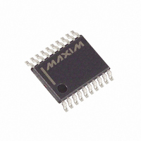
MAX3001EEUP+ Maxim Integrated Products, MAX3001EEUP+ Datasheet - Page 15

MAX3001EEUP+
Manufacturer Part Number
MAX3001EEUP+
Description
IC TRANSLATOR LEVEL 8CH 20-TSSOP
Manufacturer
Maxim Integrated Products
Datasheet
1.MAX3001EEUPT.pdf
(25 pages)
Specifications of MAX3001EEUP+
Logic Function
Translator, Bidirectional, Unidirectional, 3-State
Number Of Bits
8
Input Type
CMOS
Output Type
CMOS
Data Rate
35Mbps
Number Of Channels
8
Number Of Outputs/channel
1
Differential - Input:output
No/No
Propagation Delay (max)
8.5ns
Voltage - Supply
1.65 V ~ 5.5 V
Operating Temperature
-40°C ~ 85°C
Package / Case
20-TSSOP
Supply Voltage
1.2 V ~ 5.5 V
Logic Type
CMOS
Input Bias Current (max)
0.01 mA
Propagation Delay Time
15 ns
Supply Voltage (max)
5.5 V
Supply Voltage (min)
1.65 V
Maximum Operating Temperature
+ 85 C
Minimum Operating Temperature
- 40 C
Maximum Power Dissipation
559 mW
Mounting Style
SMD/SMT
Lead Free Status / RoHS Status
Lead free / RoHS Compliant
The MAX3000E/MAX3001E/MAX3002–MAX3012 logic-
level translators provide the level shifting necessary to
allow data transfer in a multivoltage system. Externally
applied voltages, V
either side of the device. Logic signals present on the
V
signal on the V
The MAX3000E/MAX3001E/MAX3002/MAX3003 are
bidirectional level translators allowing data translation in
either direction (V
These devices use an architecture specifically
designed to be bidirectional without the use of a direc-
tion pin. The MAX3004–MAX3012 unidirectional level
translators level shift data in one direction (V
V
MAX3000E/MAX3001E/ MAX3002–MAX3012 accept V
from +1.2V to +5.5V. All devices have V
from +1.65V to +5.5V, making them ideal for data trans-
fer between low-voltage ASICs/PLDs and higher volt-
age systems.
The MAX3000E/MAX3001E/MAX3002/MAX3004–
MAX3012 feature an output enable mode that reduces
V
current to less than 2µA when in shutdown. The
MAX3000E/MAX3001E have ±15kV ESD protection on
the V
route signals externally. The MAX3000E operates at a
guaranteed data rate of 230kbps; the MAX3001E oper-
ates at a guaranteed data rate of 4Mbps and the
MAX3002–MAX3012 are guaranteed with a data rate of
20Mbps of operation over the entire specified operating
voltage range.
For proper operation, ensure that +1.65V ≤ V
+1.2V ≤ V
sequencing, V
During power-supply sequencing, when V
and V
sourced to each load on the V
not latch up.
The maximum data rate also depends heavily on the
load capacitance (see the Typical Operating
Characteristics ), output impedance of the driver, and
the operational voltage range (see the Timing
Characteristics table).
The MAX3001E/MAX3002–MAX3012 architecture is
based on a one-shot accelerator output stage. See
Figure 5. Accelerator output stages are always in three-
L
CC
CC
side of the device appear as a higher voltage logic
supply current to less than 2µA, and V
CC
L
→ V
+1.2V to +5.5V, ±15kV ESD-Protected, 0.1µA,
is powering up, up to 10mA current can be
side for greater protection in applications that
L
≤ +5.5V, and V
L
) on any single data line. The
L
CC
≥ V
______________________________________________________________________________________
L
side of the device, and vice-versa.
CC
CC
↔ V
Input Driver Requirements
Detailed Description
and V
does not damage the device.
CC
35Mbps, 8-Channel Level Translators
L
) on any single data line.
L
L
≤ V
, set the logic levels on
side, yet the device does
Level Translation
CC
. During power-up
CC
CC
CC
L
→ V
is floating
L
≤ +5.5V,
ranging
supply
CC
or
L
state except when there is a transition on any of the
translators on the input side, either I/O V
When there is such a transition, the accelerator stages
become active, charging (discharging) the capacitances
at the I/Os. Due to its bidirectional nature, both stages
become active during the one-shot pulse. This can lead
to some current feeding into the external source that is
driving the translator. However, this behavior helps to
speed up the transition on the driven side.
For proper full-speed operation, the output current
of a device that drives the inputs of the MAX3000E/
MAX3001E/MAX3002–MAX3012 should meet the fol-
lowing requirements:
• MAX3000E (230kbps):
• MAX3001E (4Mbps):
• MAX3002–MAX3012 (20Mbps):
where i is the driver output current, V is the logic-supply
voltage (i.e., V
tance of the signal line.
The MAX3000E/MAX3001E/MAX3002 and the MAX3004–
MAX3012 feature an EN input, and the MAX3003 has an
EN A/B input. Pull EN low to set the MAX3000E/
MAX3001E/MAX3002/MAX3004–MAX3012s’ I/O V
through I/O V
V
Drive EN to logic-high (V
MAX3003 is intended for bus multiplexing or bus switch-
ing applications. Drive EN A/B low to place channels 1B
through 4B in active mode, while channels 1A through
4A are in three-state mode. Drive EN A/B to logic-high
(V
1B through 4B remain in three-state mode.
As with all Maxim devices, ESD-protection structures
are incorporated on all pins to protect against electro-
static discharges encountered during handling and
assembly. The I/O V
against static discharge. Maxim’s engineers have
developed state-of-the-art structures to protect these
pins against ESD of ±15kV without damage. The ESD
structures withstand high ESD in all states: normal
operation, three-state output mode, and powered
down. After an ESD event, Maxim’s E versions keep
working without latchup, whereas competing products
can latch and must be powered down to remove
latchup.
L
L
1 through I/O V
i > 1mA, R
i > 10
i > 10
) to enable channels 1A through 4A, while channels
7
8
x V x (C + 10pF)
x V x (C + 10pF)
Enable Output Mode (EN, EN A/B)
drv
CC
L
8 in three-state output mode, while I/O
or V
< 1kΩ
L
8 have internal 6kΩ pulldown resistors.
CC
CC
) and C is the parasitic capaci-
L
lines have extra protection
±15kV ESD Protection
) for normal operation. The
L
or I/O V
CC
.
CC
15
1


