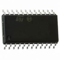
74LVX3245MTR STMicroelectronics, 74LVX3245MTR Datasheet

74LVX3245MTR
Specifications of 74LVX3245MTR
Available stocks
Related parts for 74LVX3245MTR
74LVX3245MTR Summary of contents
Page 1
... The A-port interfaces with the 3V bus, the B-port with the 5V bus. All inputs are equipped with protection circuits against static discharge, giving them 2KV ESD immunity and transient excess voltage. 74LVX3245 SOP TSSOP PACKAGE T & R SOP 74LVX3245MTR TSSOP 74LVX3245TTR Rev. 4 1/13 ...
Page 2
Figure 2: Input And Output Equivalent Circuit Table 3: Truth Table INPUTS Don’t Care Z : High Impedance Table 4: Absolute Maximum Ratings Symbol V Supply Voltage CCA V Supply Voltage CCB V ...
Page 3
Table 5: Recommended Operating Conditions Symbol V Supply Voltage (note 1) CCA V Supply Voltage (note 1) CCB V Input Voltage I V I/O Voltage I/OA V I/O Voltage I/OB T Operating Temperature op dt/dv Input Rise and Fall Time ...
Page 4
Table 7: DC Specifications For V Symbol Parameter V CCA (V) V High Level Input 3.3 IHB Voltage 3.3 V Low Level Input 3.3 ILB Voltage 3.3 V High Level 3.0 OHB Output Voltage 3.3 V Low Level Output ...
Page 5
Table 9: AC Electrical Characteristics (C Symbol Parameter V t Propagation Delay PLH Time (An to Bn) 3.0 t Propagation Delay PHL Time (An to Bn) 3.0 t Output Enable PZL Time (G to Bn) 3.0 t Output Enable PZH ...
Page 6
Table 10: Capacitive Characteristics Symbol Parameter V CCA (V) C Input open open IN Capacitance C Input/Output 3.3 I/O Capacitance C Dynamic Low 3.3 PD Level Quiet Output (note Dynamic Low 3.3 PD Level ...
Page 7
Figure 4: Waveform - Propagation Delays (f=1MHz; 50% duty cycle) Figure 5: Waveform - Output Enable And Disable Time (f=1MHz; 50% duty cycle) 74LVX3245 7/13 ...
Page 8
DIM. MIN. A 2.35 A1 0.1 B 0.33 C 0.23 D 15. 10.00 h 0.25 L 0.4 k 0° ddd 8/13 SO-24 MECHANICAL DATA mm. TYP MAX. 2.65 0.30 0.51 0.32 15.60 7.6 1.27 10.65 ...
Page 9
TSSOP24 MECHANICAL DATA DIM. MIN 0. 0.19 c 0.09 D 7 6.25 K 0° PIN 1 IDENTIFICATION 1 mm. TYP MAX. 1.1 0.15 0.9 0.30 0.20 ...
Page 10
DIM. MIN 12 10.8 Bo 15.7 Ko 2.9 Po 3.9 P 11.9 10/13 Tape & Reel SO-24 MECHANICAL DATA mm. TYP MAX. 330 13.2 30.4 11.0 15.9 3.1 4.1 12.1 inch ...
Page 11
Tape & Reel TSSOP24 MECHANICAL DATA DIM. MIN 12 6.8 Bo 8.2 Ko 1.7 Po 3.9 P 11.9 mm. TYP MAX. 330 13.2 0.504 0.795 2.362 22.4 7 0.268 8.4 0.323 1.9 ...
Page 12
Table 11: Revision History Date Revision 27-Aug-2004 4 12/13 Description of Changes Ordering Codes Revision - pag. 1. ...
Page 13
... No license is granted by implication or otherwise under any patent or patent rights of STMicroelectronics. Specifications mentioned in this publication are subject to change without notice. This publication supersedes and replaces all information previously supplied. STMicroelectronics products are not authorized for use as critical components in life support devices or systems without express written approval of STMicroelectronics ...


