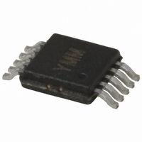
SY55855VKG Micrel Inc, SY55855VKG Datasheet - Page 5

SY55855VKG
Manufacturer Part Number
SY55855VKG
Description
IC TRANSLATOR DUAL LVDS 10MSOP
Manufacturer
Micrel Inc
Series
SY55r
Datasheet
1.SY55855VKG.pdf
(8 pages)
Specifications of SY55855VKG
Logic Function
Translator
Number Of Bits
2
Input Type
CML, PECL, LVPECL
Output Type
LVDS
Data Rate
1.5Gbps
Number Of Channels
2
Number Of Outputs/channel
1
Differential - Input:output
Yes/Yes
Propagation Delay (max)
0.7ns
Voltage - Supply
3 V ~ 5.7 V
Operating Temperature
-40°C ~ 85°C
Package / Case
10-MSOP, Micro10™, 10-uMAX, 10-uSOP
Supply Voltage
3 V ~ 5.7 V
Logic Family
ECL
Logical Function
Translator
Technology
ECL
High Level Output Current
-4mA
Low Level Output Current
4mA
Operating Supply Voltage (min)
3V
Abs. Propagation Delay Time
700ps
Mounting
Surface Mount
Operating Temperature (min)
-40C
Operating Temperature (max)
85C
Operating Temperature Classification
Industrial
Lead Free Status / RoHS Status
Lead free / RoHS Compliant
Other names
576-1376
Available stocks
Company
Part Number
Manufacturer
Quantity
Price
Company:
Part Number:
SY55855VKG
Manufacturer:
MICREL
Quantity:
1 800
Company:
Part Number:
SY55855VKG TR
Manufacturer:
ST
Quantity:
212
Company:
Part Number:
SY55855VKGTR
Manufacturer:
MICREL
Quantity:
162
Micrel, Inc.
Note 1.
V
V
V
Note 2.
Note 3.
Note 4.
Note 5.
M9999-110705
hbwhelp@micrel.com or (408) 955-1690
Symbol
V
I
Symbol
V
V
V
Symbol
V
V
V
V
CC
CC
CC
CC
ABSOLUTE MAXIMUM RATINGS
DC ELECTRICAL CHARACTERISTICS
CML DC ELECTRICAL CHARACTERISTICS
LVDS DC ELECTRICAL CHARACTERISTICS
CC
ID
IH
IL
OD
OCM
V
OH
OL
V
V
I
T
T
T
OUT
OCM
A
LEAD
store
CC
IN
= 3.0V to 5.7V; GND = 0V; T
= 3.0V to 5.7V; GND = 0V; T
= 3.0V to 5.7V; GND = 0V; T
Symbol
Permanent device damage may occur if absolute maximum ratings are exceeded. This is a stress rating only and functional operation is not
implied at conditions other than those detailed in the operational sections of this data sheet. Exposure to absolute maximum ratlng conditions
for extended periods may affect device reliability.
Equilibrium temperature.
Measured as per Figure 4.
Measured as per Figure 3.
Do not short output to GND.
Differential Output Voltage
Output Common Mode
Voltage
Change in Common Mode
Voltage
Output HIGH Voltage
Output LOW Voltage
Power Supply Voltage
Power Supply Current
Differential Input Voltage
Input HIGH Voltage
Input LOW Voltage
Parameter
Parameter
Parameter
(3)
(3)
3.6V <V
V
Power Supply Voltage
Input Voltage
LVDS Output Current
Operating Temperature Range
Lead Temperature (soldering, 20sec.)
Storage Temperature Range
CC
CC
(4), (5)
(4), (5)
<5.7V
3.6V
A
A
A
(4)
= –40 C to +85 C
= –40 C to +85 C
= –40 C to +85 C
Min.
3.0
—
—
T
1.125
0.925
Min.
Min.
100
250
–50
1.6
1.5
(1)
A
—
= –40 C
Rating
Max.
5.7
80
50
(2)
(2)
(2)
5
Typ.
Typ.
Min.
—
—
—
—
—
—
—
—
3.0
—
—
T
A
= +25 C
Typ.
30
—
—
V
CC
1.375
1.474
Max.
Max.
V
450
+50
—
—
CC
– 0.1
Max.
5.7
80
50
–0.5 to V
–0.5 to +6.0
–65 to +150
–40 to +85
Unit
Unit
Value
mV
mV
mV
260
V
V
V
V
V
10%
CC
Min.
3.0
T
—
—
+0.5
A
= +85 C
100 Termination
I
OH
I
OL
Condition
Condition
Max.
5.7
= –4.0mA
80
50
= 4.0mA
SuperLite™
Unit
SY55855V
mA
V
V
C
C
C
Unit
mA
V


