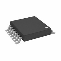
ADG3304BRUZ Analog Devices Inc, ADG3304BRUZ Datasheet - Page 16

ADG3304BRUZ
Manufacturer Part Number
ADG3304BRUZ
Description
IC XLATOR 4CH 1.2/5.5V 14-TSSOP
Manufacturer
Analog Devices Inc
Datasheet
1.ADG3304BRUZ.pdf
(20 pages)
Specifications of ADG3304BRUZ
Logic Function
Translator, Bidirectional
Number Of Bits
4
Input Type
Logic
Output Type
Logic
Data Rate
50Mbps
Number Of Channels
4
Number Of Outputs/channel
1
Differential - Input:output
No/No
Propagation Delay (max)
6ns
Voltage - Supply
1.15 V ~ 5.5 V
Operating Temperature
-40°C ~ 85°C
Package / Case
14-TSSOP
Supply Voltage
1.5 V ~ 5.5 V
No. Of Inputs
4
Propagation Delay
6ns
Logic Type
Level Translator
Supply Voltage Range
1.15V To 5.5V
Logic Case Style
TSSOP
No. Of Pins
14
Operating Temperature Range
-40°C To +85°C
Lead Free Status / RoHS Status
Lead free / RoHS Compliant
Available stocks
Company
Part Number
Manufacturer
Quantity
Price
Company:
Part Number:
ADG3304BRUZ
Manufacturer:
ADI
Quantity:
3 000
Part Number:
ADG3304BRUZ
Manufacturer:
ADI/亚德诺
Quantity:
20 000
ADG3304
THEORY OF OPERATION
The ADG3304 level translator allows the level shifting
necessary for data transfer in a system where multiple supply
voltages are used. The device requires two supplies, V
V
side of the device. When driving the A pins, the device translates
the V
available at the Y pins. Similarly, because the device is capable of
bidirectional translation, when driving the Y pins, the V
compatible logic levels are translated to V
levels available at the A pins. When EN = 0, Pin A1 to Pin A4
and Pin Y1 to Pin Y4 are three-stated. When EN is driven high,
the ADG3304 goes into normal operation mode and performs
level translation.
LEVEL TRANSLATOR ARCHITECTURE
The ADG3304 consists of four bidirectional channels. Each
channel can translate logic levels in either the A→Y or the Y→A
direction. It uses a one-shot accelerator architecture, which
ensures excellent switching characteristics. Figure 39 shows a
simplified block diagram of a bidirectional channel.
The logic level translation in the A→Y direction is performed
using a level translator (U1) and an inverter (U2), while the
translation in the Y→A direction is performed using Inverter U3
and Inverter U4. The one-shot generator detects a rising or
falling edge present on either the A side or the Y side of the
channel. It sends a short pulse that turns on the PMOS
transistors (T1 to T2) for a rising edge, or the NMOS transistors
(T3 to T4) for a falling edge. This charges/discharges the
capacitive load faster, which results in faster rise and fall times.
The inputs of the unused channels (A or Y) should be tied to
their corresponding V
CCY
(V
CCA
Figure 39. Simplified Block Diagram of an ADG3304 Channel
CCA
-compatible logic levels to V
A
≤ V
T1
T4
V
CCA
CCY
). These supplies set the logic levels on each
6kΩ
P
ONE-SHOT GENERATOR
CC
U1
rail (V
U4
U2
CCA
U3
or V
CCY
6kΩ
CCY
-compatible logic levels
CCA
N
) or to GND.
-compatible logic
V
CCY
T3
T2
CCA
Y
CCY
and
-
Rev. B | Page 16 of 20
INPUT DRIVING REQUIREMENTS
To ensure correct operation of the ADG3304, the circuit that
drives the input of the ADG3304 channels should have an
output impedance of less than or equal to 150 Ω and a
minimum peak current driving capability of 36 mA.
OUTPUT LOAD REQUIREMENTS
The ADG3304 level translator is designed to drive CMOS-
compatible loads. If current-driving capability is required, it is
recommended to use buffers between the ADG3304 outputs
and the load.
ENABLE OPERATION
The ADG3304 provides three-state operation at the A and Y
I/O pins by using the enable pin (EN), as shown in Table 5.
Table 5. Truth Table
EN
0
1
1
2
While EN = 0, the ADG3304 enters into three-state mode. In this
mode, the current consumption from both the V
supplies is reduced, allowing the user to save power, which is
critical, especially on battery-operated systems. The EN input pin
can be driven with either V
logic levels.
POWER SUPPLIES
For proper operation of the ADG3304, the voltage applied to
the V
To meet this condition, the recommended power-up sequence
is V
only after both supply voltages reach their nominal values. It is
not recommended to use the part in a system where, during
power-up, V
increase in the current taken from the V
optimum performance, the V
decoupled to GND as close as possible to the device.
High impedance state.
In normal operation, the ADG3304 performs level translation.
CCY
CCA
first and then V
must be less than or equal to the voltage applied to V
CCA
Y I/O Pins
Hi-Z
Normal operation
can be greater than V
1
CCA
CCA
. The ADG3304 operates properly
-compatible or V
CCA
pin and V
2
CCY
A I/O Pins
Hi-Z
Normal operation
CCA
due to a significant
1
CCY
supply. For
CCY
CCA
pin should be
-compatible
and V
CCY
2
CCY
.


