FXL4T245BQX Fairchild Semiconductor, FXL4T245BQX Datasheet - Page 3
FXL4T245BQX
Manufacturer Part Number
FXL4T245BQX
Description
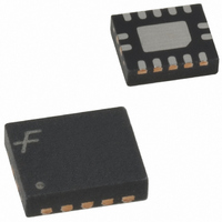
TRANSLATOR 4BIT DUAL LV 14DQFN
Manufacturer
Fairchild Semiconductor
Datasheet
1.FXL4T245BQX.pdf
(9 pages)
Specifications of FXL4T245BQX
Logic Function
Translator, Bidirectional, 3-State
Number Of Bits
4
Input Type
Voltage
Output Type
Voltage
Number Of Channels
1
Number Of Outputs/channel
1
Differential - Input:output
No/No
Propagation Delay (max)
3.5ns
Voltage - Supply
1.1 V ~ 3.6 V
Operating Temperature
-40°C ~ 85°C
Package / Case
14-WQFN Exposed Pad, 14-DQFN
Supply Voltage
1.1 V ~ 3.6 V
Logic Type
Translator
Logic Family
FXL
Input Bias Current (max)
0.01 mA
High Level Output Current
- 24 mA
Low Level Output Current
24 mA
Propagation Delay Time
24 ns @ 1.1 V to 1.3 V
Supply Voltage (max)
3.6 V
Supply Voltage (min)
1.1 V
Maximum Operating Temperature
+ 85 C
Minimum Operating Temperature
- 40 C
Maximum Power Dissipation
20 pF
Mounting Style
SMD/SMT
Lead Free Status / RoHS Status
Lead free / RoHS Compliant
Data Rate
-
Lead Free Status / Rohs Status
Lead free / RoHS Compliant
Other names
FXL4T245BQXTR
FXL4T245BQX_NL
FXL4T245BQX_NLTR
FXL4T245BQX_NLTR
FXL4T245BQX_NL
FXL4T245BQX_NLTR
FXL4T245BQX_NLTR
Available stocks
Company
Part Number
Manufacturer
Quantity
Price
Company:

Part Number:
FXL4T245BQX
Manufacturer:
FSC
Quantity:
7 860


V
(Note 4)
V
(Note 4)
Absolute Maximum Ratings
DC Electrical Characteristics
Supply Voltage
DC Input Voltage (V
Output Voltage (V
DC Input Diode Current (I
DC Output Diode Current (I
DC Output Source/Sink Current
DC V
Storage Temperature Range (T
IH
IL
Symbol
V
V
I/O Port A
I/O Port B
Control Inputs (T/R, OE)
Outputs 3-STATE
Outputs Active (A
Outputs Active (B
V
V
(I
Supply Pin (I
CCA
CCB
O
O
OH
CC
/I
OL
0V
V
or Ground Current per
CC
)
High Level Input Voltage
Low Level Input Voltage
CC
)
O
) (Note 2)
n
n
I
)
)
)
Parameter
IK
) V
OK
)
I
STG
0V
)
0.5V to V
0.5V to V
50 mA / 50 mA
65 C to 150 C
Data Inputs A
Control Pins/OE, T/R
(Referenced to V
Data Inputs A
Control Pins/OE, T/R
(Referenced to V
(Note 1)
0.5V to 4.6V
0.5V to 4.6V
0.5V to 4.6V
0.5V to 4.6V
0.5V to 4.6V
0.5V to 4.6V
CCA
CCB
100 mA
Conditions
50 mA
50 mA
50 mA
0.5V
0.5V
n
n
, B
, B
CCA
CCA
n
n
3
Recommended Operating
Conditions
Note 1: The “Absolute Maximum Ratings” are those values beyond which
the safety of the device cannot be guaranteed. The device should not be
operated at these limits. The parametric values defined in the Electrical
Characteristics tables are not guaranteed at the absolute maximum ratings.
The “Recommended Operating Conditions” table will define the conditions
for actual device operation.
Note 2: I
Note 3: All unused inputs must be held at V
Power Supply Operating (V
Input Voltage
Output Current in I
Free Air Operating Temperature (T
Minimum Input Edge Rate ( V/ t)
)
)
Port A
Port B
Control Inputs (T/R, OE)
V
3.0V to 3.6V
2.3V to 2.7V
1.65V to 1.95V
1.4V to 1.65V
1.1V to 1.4V
V
CC
CCA/B
O
Absolute Maximum Rating must be observed.
1.65 - 2.3
1.4 - 1.65
1.65 - 2.3
1.4 - 1.65
1.65 - 2.3
1.4 - 1.65
1.65 - 2.3
1.4 - 1.65
2.7 - 3.6
2.3 - 2.7
1.1 - 1.4
2.7 - 3.6
2.3 - 2.7
1.1 - 1.4
2.7 - 3.6
2.3 - 2.7
1.1 - 1.4
2.7 - 3.6
2.3 - 2.7
1.1 - 1.4
V
(V)
1.1V to 3.6V
CCI
OH
(Note 3)
1.1 - 3.6
1.1 - 3.6
1.1 - 3.6
1.1 - 3.6
V
/I
(V)
CCO
OL
CCA
0.65 x V
0.65 x V
0.65 x V
0.65 x V
0.9 x V
0.9 x V
or V
Min
2.0
1.6
2.0
1.6
CCI
A
CCA
CCB
)
CCI
CCA
CCA
CCI
CCI
or GND.
www.fairchildsemi.com
)
0.35 x V
0.35 x V
0.35 x V
0.35 x V
0.1 x V
0.1 x V
Max
0.8
0.7
0.8
0.7
40 C to 85 C
0.0V to V
CCA
1.1V to 3.6V
0.0V to 3.6V
0.0V to 3.6V
CCI
CCA
CCA
CCI
CCI
10 ns/V
0.5 mA
24 mA
18 mA
Units
6 mA
2 mA
V
V
CCA
Related parts for FXL4T245BQX
Image
Part Number
Description
Manufacturer
Datasheet
Request
R

Part Number:
Description:
Fairchild Semiconductor [IGBT MODULE]
Manufacturer:
Fairchild Semiconductor
Datasheet:

Part Number:
Description:
Discrete Semiconductor Modules
Manufacturer:
Fairchild Semiconductor
Part Number:
Description:
Discrete Semiconductor Modules
Manufacturer:
Fairchild Semiconductor
Part Number:
Description:
This N-Channel MOSFET is produced using Fairchild Semiconductor’s advanced Power Trench® process
Manufacturer:
Fairchild Semiconductor
Datasheet:
Part Number:
Description:
This N-Channel MOSFET is produced using Fairchild Semiconductor’s advanced Power Trench® process
Manufacturer:
Fairchild Semiconductor
Datasheet:
Part Number:
Description:
This N-Channel MOSFET is produced using Fairchild Semiconductor’s advanced PowerTrench® process
Manufacturer:
Fairchild Semiconductor
Datasheet:
Part Number:
Description:
This N-Channel MOSFET is produced using Fairchild Semiconductor’s advanced PowerTrench® process
Manufacturer:
Fairchild Semiconductor
Datasheet:
Part Number:
Description:
This N-Channel MOSFET is produced using Fairchild Semiconductor’s advanced Power Trench® process
Manufacturer:
Fairchild Semiconductor
Datasheet:
Part Number:
Description:
This N-Channel logic Level MOSFETs are produced using Fairchild Semiconductor‘s advanced Power Trench® process that has been special tailored to minimize the on-state resistance and yet maintain superior switching performance
Manufacturer:
Fairchild Semiconductor
Datasheet:
Part Number:
Description:
This N-Channel MOSFET is produced using Fairchild Semiconductor’s advanced Power Trench® process
Manufacturer:
Fairchild Semiconductor
Datasheet:
Part Number:
Description:
This N-Channel SyncFET™ is produced using Fairchild Semiconductor’s advanced PowerTrench® process
Manufacturer:
Fairchild Semiconductor
Datasheet:
Part Number:
Description:
This N-Channel SyncFET™ is produced using Fairchild Semiconductor’s advanced PowerTrench® process
Manufacturer:
Fairchild Semiconductor
Datasheet:
Part Number:
Description:
This N-Channel SyncFET™ is produced using Fairchild Semiconductor’s advanced PowerTrench® process
Manufacturer:
Fairchild Semiconductor
Datasheet:
Part Number:
Description:
This N-Channel logic Level MOSFETs are produced using Fairchild Semiconductor‘s advanced Power Trench® process that has been special tailored to minimize the on-state resistance and yet maintain superior switching performance
Manufacturer:
Fairchild Semiconductor
Datasheet:
Part Number:
Description:
This N-Channel MOSFET is produced using Fairchild Semiconductor’s advanced Power Trench® process that has been especially tailored to minimize the on-state resistance and yet maintain superior switching performance
Manufacturer:
Fairchild Semiconductor
Datasheet: