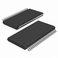
IDT74FST1632861PAG IDT, Integrated Device Technology Inc, IDT74FST1632861PAG Datasheet - Page 4

IDT74FST1632861PAG
Manufacturer Part Number
IDT74FST1632861PAG
Description
IC BUS SWTCH 20BIT 2PORT 48TSSOP
Manufacturer
IDT, Integrated Device Technology Inc
Series
74FSTr
Type
Bus Switchr
Datasheet
1.IDT74FST1632861PAG8.pdf
(6 pages)
Specifications of IDT74FST1632861PAG
Circuit
2 x 10:10
Independent Circuits
2
Voltage Supply Source
Single Supply
Operating Temperature
-40°C ~ 85°C
Mounting Type
Surface Mount
Package / Case
48-TSSOP
Lead Free Status / RoHS Status
Lead free / RoHS Compliant
Voltage - Supply
-
Current - Output High, Low
-
Other names
74FST1632861PAG
SWITCHING CHARACTERISTICS OVER OPERATING RANGE
Following Conditions Apply Unless Otherwise Specified:
Industrial: T
NOTES:
1. See test circuits and waveforms.
2. The bus switch contributes no Propagation Delay other than the RC Delay of the load interacting with the RC of the switch.
3. |Q
POWER SUPPLY CHARACTERISTICS
NOTES:
1. For conditions shown as Max. or Min., use appropriate value specified under Electrical Characteristics for the applicable device type. T
2. Typical values are at V
3. Per TTL driven input (V
4. This parameter represents the current required to switch the internal capacitance of the control inputs at the specified frequency.
5. C
6. I
IDT74FST1632861
20-BIT, TWO PORT BUS SWITCH WITH RESISTOR
Symbol
Symbol
port switches from one path to another. Charge injection is reduced because the injection from the DISCONNECT of the first path is compensated by the CONNECT of the
second path.
Switch inputs generate no significant power supply currents as they transition. This parameter is not directly testable, but is derived for use in Total Power Supply Calculations.
C
I
I
ΔI
D
N
I
f
N = Number of Control Inputs Toggling at f
C
C
CC
CCD
i
PD
PD
H
T
|Q
ΔI
I
= Control Input Frequency
CI
CC
t
t
t
t
t
t
CCD
= I
= I
PZH
PHZ
PLH
PHL
PZL
PLZ
I
= Number of TTL Inputs at D
| is the charge injection for a single switch DISCONNECT and applies to either single switches or multiplexers. |Q
C
= Duty Cycle for TTL Inputs High
CC
= Quiescent Current
CI
= I
= Power Dissipation Capacitance
QUIESCENT
CC
= Dynamic Current Caused by an Input Transition Pair (HLH or LHL)
= Power Supply Current for a TTL High Input (V
|
CCD
+ ΔI
A
/V
CC
= -40°C to +85°C, V
CC
Quiescent Power Supply Current
TTL Inputs HIGH
Dynamic Power Supply
Current
Total Power Supply Current
Description
Data Propagation Delay
A to B, Y to B
Switch CONNECT Delay
xOE to A or B
Switch DISCONNECT Delay
xOE to A or B
Charge Injection During Switch DISCONNECT,
xOE to A or B
+ I
D
H
INPUTS
N
T
+ I
(4,5)
CC
+ I
IN
CCD
= 3.4V). All other inputs at V
DYNAMIC
= 5.0V, +25°C ambient.
Parameter
(1)
(f
(2)
(3)
i
N)
H
CC
= 5.0V ± 10%
i
(6)
IN
CC
= 3.4V)
V
V
V
Outputs Open
Select Input Togging
50% Duty Cycle
V
Outputs Open
Two Enable Pins Toggling
f
50% Duty Cycle
i
or GND. Switch inputs do not contribute to ΔI
IN
CC
CC
CC
= 10MHz
= 3.4V
= Max.
= Max.
= Max.
(3)
Test Conditions
4
Min.
1.5
1.5
—
—
V
V
V
V
V
V
(1)
V
IN
IN
IN
IN
IN
IN
CC
= V
= V
= 3.4V
= GND
= GND
= GND
= 5V ± 10%
CC
CC
Typ.
CC.
1.5
—
—
—
DCI
| is the charge injection for a multiplexer as the multiplexed
Max.
0.25
6.5
—
7
INDUSTRIAL TEMPERATURE RANGE
Min.
—
—
—
—
A
Typ.
= –40°C to +85°C
0.5
0.6
0.7
V
30
CC
Max.
(2)
0.25
—
7
7
= 4V
Max.
400
1.5
9.5
8
Select
MHz/
Unit
µA/
mA
mA
Unit
pC
ns
ns
ns


