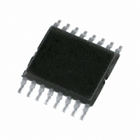
74LVC139PW,118 NXP Semiconductors, 74LVC139PW,118 Datasheet - Page 2

74LVC139PW,118
Manufacturer Part Number
74LVC139PW,118
Description
IC DUAL 2-4 DECOD/DEMUX 16-TSSOP
Manufacturer
NXP Semiconductors
Series
74LVCr
Type
Decoder/Demultiplexerr
Datasheet
1.74LVC139BQ115.pdf
(17 pages)
Specifications of 74LVC139PW,118
Package / Case
16-TSSOP
Circuit
1 x 2:4
Independent Circuits
2
Current - Output High, Low
24mA, 24mA
Voltage Supply Source
Single Supply
Voltage - Supply
2.7 V ~ 3.6 V
Operating Temperature
-40°C ~ 125°C
Mounting Type
Surface Mount
Logic Family
LVC
Number Of Lines (input / Output)
2.0 / 4.0
Propagation Delay Time
50 ns
Supply Voltage (max)
3.6 V
Supply Voltage (min)
1.2 V
Maximum Operating Temperature
+ 125 C
Minimum Operating Temperature
- 40 C
Mounting Style
SMD/SMT
Number Of Input Lines
2.0
Number Of Output Lines
4.0
Lead Free Status / RoHS Status
Lead free / RoHS Compliant
Lead Free Status / RoHS Status
Lead free / RoHS Compliant, Lead free / RoHS Compliant
Other names
568-4492-2
74LVC139PW-T
74LVC139PW-T
935196010118
74LVC139PW-T
74LVC139PW-T
935196010118
Available stocks
Company
Part Number
Manufacturer
Quantity
Price
Company:
Part Number:
74LVC139PW,118
Manufacturer:
NXP Semiconductors
Quantity:
4 000
Philips Semiconductors
FEATURES
QUICK REFERENCE DATA
GND = 0 V; T
Notes
1. C
2. The condition is V
2004 Mar 15
C
C
t
PHL
SYMBOL
Wide supply voltage range from 1.2 V to 3.6 V
Inputs accept voltages up to 5.5 V
CMOS low power consumption
Direct interface with TTL levels
Demultiplexing capability
Two independent 2-to-4 decoders
Multifunction capability
Active LOW mutually exclusive outputs
Output drive capability 50
125 C
In accordance with JEDEC standard no. 8-1A
ESD protection:
HBM EIA/JESD22-A114-A exceeds 2000 V
MM EIA/JESD22-A115-A exceeds 200 V.
I
PD
Dual 2-to-4 line decoder/demultiplexer
P
f
f
C
V
N = total load switching outputs;
i
o
(C
/t
D
CC
PD
= input frequency in MHz;
L
= output frequency in MHz;
PLH
= output load capacitance in pF;
= C
L
is used to determine the dynamic power dissipation (P
= supply voltage in Volts;
PD
V
CC
amb
propagation delay
input capacitance
power dissipation capacitance per multiplexer V
2
V
nA to nYn
nE to nYn
CC
= 25 C; t
f
o
2
) = sum of the outputs.
I
f
= GND to V
i
N + (C
r
= t
f
transmission lines at
PARAMETER
2.5 ns.
L
CC
.
V
CC
2
f
o
) where:
2
DESCRIPTION
The 74LVC139 is a high-performance, low-voltage and
low-power Si-gate CMOS device, superior to most
advanced CMOS compatible TTL families.
The 74LVC139 is a dual 2-to-4 line decoder/demultiplexer.
This device has two independent decoders, each
accepting two binary weighted inputs (nA0 and nA1) and
providing four mutually exclusive active LOW outputs
(nY0 to nY3). Each decoder has an active LOW input (nE).
When nE is HIGH, every output is forced HIGH. The
enable input can be used as the data input for a 1-to-4
demultiplexer application.
C
D
CC
L
in W).
= 50 pF; V
= 3.3 V; notes 1 and 2 17
CONDITIONS
CC
= 3.3 V
2.9
2.7
5.0
TYPICAL
Product specification
74LVC139
ns
ns
pF
pF
UNIT


