IDT74CBTLV3253PGG IDT, Integrated Device Technology Inc, IDT74CBTLV3253PGG Datasheet - Page 2
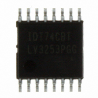
IDT74CBTLV3253PGG
Manufacturer Part Number
IDT74CBTLV3253PGG
Description
IC MUX/DEMUX 1:4 DUAL LV 16TSSOP
Manufacturer
IDT, Integrated Device Technology Inc
Series
74CBTLVr
Type
Multiplexer/Demultiplexerr
Datasheet
1.IDT74CBTLV3253QG.pdf
(5 pages)
Specifications of IDT74CBTLV3253PGG
Circuit
1 x 2:4
Independent Circuits
1
Current - Output High, Low
15mA, 64mA
Voltage Supply Source
Single Supply
Voltage - Supply
2.3 V ~ 3.6 V
Operating Temperature
-40°C ~ 85°C
Mounting Type
Surface Mount
Package / Case
16-TSSOP
Configuration
2 x 4:1
Number Of Inputs
8
Number Of Outputs
2
Operating Supply Voltage (typ)
2.5/3.3V
Operating Supply Voltage (min)
2.3V
Operating Supply Voltage (max)
3.6V
Operating Temp Range
-40C to 85C
Operating Temperature Classification
Industrial
Mounting
Surface Mount
Pin Count
16
Package Type
TSSOP
Lead Free Status / RoHS Status
Lead free / RoHS Compliant
Other names
74CBTLV3253PGG
800-1568
800-1568-5
800-1568
800-1568
800-1568-5
800-1568


PIN CONFIGURATION
OPERATING CHARACTERISTICS, T
NOTE:
1. All unused control inputs of the device must be held at V
SIMPLIFIED SCHEMATIC, EACH
SWITCH
IDT74CBTLV3253
LOW-VOLTAGE DUAL 1-OF-4 MULTIPLEXER/DEMULTIPLEXER
Symbol
V
V
V
T
CC
IH
IL
A
Parameter
Supply Voltage
High-Level Control Input Voltage
Low-Level Control Input Voltage
Operating Free-Air Temperature
GND
1OE
A
1B4
1B3
1B2
1B1
S1
1A
1
8
2
3
4
5
6
7
QSOP / TSSOP
TOP VIEW
CIRCUITRY
CONTROL
16
15
14
13
12
11
10
9
CC
or GND to ensure proper device operation.
2A
V
2OE
S0
2B4
2B3
2B2
2B1
CC
B
Test Conditions
V
V
V
V
CC
CC
CC
CC
A
= 2.3V to 2.7V
= 2.7V to 3.6V
= 2.3V to 2.7V
= 2.7V to 3.6V
= 25°C
2
ABSOLUTE MAXIMUM RATINGS
FUNCTION TABLE
ONE OF TWO 1:4 MUX/DEMUX BANKS
NOTE:
1. H = HIGH Voltage Level
NOTE:
1. Stresses greater than those listed under ABSOLUTE MAXIMUM RATINGS may cause
Symbol
V
V
I
T
IK
STG
CC
permanent damage to the device. This is a stress rating only and functional operation
of the device at these or any other conditions above those indicated in the operational
sections of this specification is not implied. Exposure to absolute maximum rating
conditions for extended periods may affect reliability.
L = LOW Voltage Level
X = Don't Care
I
(1)
OE
H
L
L
L
L
SupplyVoltage Range
Input Voltage Range
Continuous Channel Current
Input Clamp Current, V
Storage Temperature
Min.
−40
Description
Inputs
2.3
1.7
—
—
2
S1
H
H
X
L
L
INDUSTRIAL TEMPERATURE RANGE
I/O
(1)
< 0
S0
H
H
Max.
X
L
L
3.6
0.7
0.8
—
—
85
–0.5 to +4.6
–0.5 to +4.6
–65 to +150
Max
128
–50
A Port = B1 Port
A Port = B2 Port
A Port = B3 Port
A Port = B4 Port
Disconnect
Function
(1)
Unit
°C
V
V
V
Unit
mA
mA
° C
V
V
Related parts for IDT74CBTLV3253PGG
Image
Part Number
Description
Manufacturer
Datasheet
Request
R

Part Number:
Description:
TRANSLATION DEVICE DPI 80-PQFP
Manufacturer:
IDT, Integrated Device Technology Inc
Datasheet:
Part Number:
Description:
IDT PART
Manufacturer:
IDT, Integrated Device Technology Inc
Datasheet:
Part Number:
Description:
IC LIU T1/E1/J1 OCTAL 256PBGA
Manufacturer:
IDT, Integrated Device Technology Inc
Datasheet:

Part Number:
Description:
IC FREQ TIMING GENERATOR 28TSSOP
Manufacturer:
IDT, Integrated Device Technology Inc
Datasheet:
Part Number:
Description:
IC CLK DVR PLL 1:10 40VFQFPN
Manufacturer:
IDT, Integrated Device Technology Inc
Datasheet:
Part Number:
Description:
IC CLK FANOUT BUFFER 1:18 32LQFP
Manufacturer:
IDT, Integrated Device Technology Inc
Datasheet:
Part Number:
Description:
IC CLK FANOUT BUFFER 1:18 32LQFP
Manufacturer:
IDT, Integrated Device Technology Inc
Datasheet:
Part Number:
Description:
IC CK505 VREG/RES 56TSSOP
Manufacturer:
IDT, Integrated Device Technology Inc
Datasheet:

Part Number:
Description:
IC SDRAM CLK DVR 1:10 48-TSSOP
Manufacturer:
IDT, Integrated Device Technology Inc
Datasheet:

Part Number:
Description:
IC CLK DVR PLL 1:10 48TSSOP
Manufacturer:
IDT, Integrated Device Technology Inc
Datasheet:
Part Number:
Description:
IC FLEXPC CLK PROGR P4 56-TSSOP
Manufacturer:
IDT, Integrated Device Technology Inc
Datasheet:
Part Number:
Description:
IC FLEXPC CLK PROGR P4 56-TSSOP
Manufacturer:
IDT, Integrated Device Technology Inc
Datasheet:
Part Number:
Description:
IC FLEXPC CLK PROGR P4 56-SSOP
Manufacturer:
IDT, Integrated Device Technology Inc
Datasheet:

Part Number:
Description:
IC PLL CLK DRIVER 2.5V 28-TSSOP
Manufacturer:
IDT, Integrated Device Technology Inc
Datasheet:
Part Number:
Description:
IC CLOCK DRIVER 2.5V 24-TSSOP
Manufacturer:
IDT, Integrated Device Technology Inc
Datasheet: