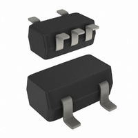
74CBTLV1G125GW,125 NXP Semiconductors, 74CBTLV1G125GW,125 Datasheet - Page 15

74CBTLV1G125GW,125
Manufacturer Part Number
74CBTLV1G125GW,125
Description
IC SINGLE BUS SWITCH 5-TSSOP
Manufacturer
NXP Semiconductors
Series
74CBTLVr
Type
FET Bus Switchr
Datasheet
1.74CBTLV1G125GV125.pdf
(21 pages)
Specifications of 74CBTLV1G125GW,125
Package / Case
SC-70-5, SC-88A, SOT-323-5, SOT-353, 5-TSSOP
Circuit
1 x 1:1
Independent Circuits
1
Voltage Supply Source
Single Supply
Voltage - Supply
2.3 V ~ 3.6 V
Operating Temperature
-40°C ~ 125°C
Mounting Type
Surface Mount
Logic Family
CBTLV
On Resistance (max)
11 Ohms
Propagation Delay Time
0.16 ns
Maximum Operating Temperature
+ 125 C
Minimum Operating Temperature
- 40 C
Function
Bus Switch
High Level Output Current
- 128 mA
Low Level Output Current
128 mA
Mounting Style
SMD/SMT
Operating Supply Voltage
2.5 V, 3.3 V
Organization
1 x 1:1
Supply Voltage (max)
3.6 V
Supply Voltage (min)
2.3 V
Logic Type
CMOS
Number Of Circuits
1
Lead Free Status / RoHS Status
Lead free / RoHS Compliant
Current - Output High, Low
-
Lead Free Status / Rohs Status
Lead free / RoHS Compliant
Other names
568-4833-2
74CBTLV1G125GW,125
74CBTLV1G125GW-G
74CBTLV1G125GW-G
935280319125
74CBTLV1G125GW,125
74CBTLV1G125GW-G
74CBTLV1G125GW-G
935280319125
NXP Semiconductors
Fig 17. Package outline SOT891 (XSON6)
74CBTLV1G125
Product data sheet
XSON6: plastic extremely thin small outline package; no leads; 6 terminals; body 1 x 1 x 0.5 mm
DIMENSIONS (mm are the original dimensions)
Note
1. Can be visible in some manufacturing processes.
UNIT
mm
VERSION
OUTLINE
SOT891
max
0.5
A
max
0.04
A
1
0.20
0.12
e
b
terminal 1
index area
6×
IEC
(1)
L
1.05
0.95
1
D
1.05
0.95
E
0
1
6
JEDEC
0.55
e
All information provided in this document is subject to legal disclaimers.
e
1
REFERENCES
D
0.35
2
5
e
1
e
Rev. 2 — 29 July 2010
1
0.35
0.27
L
b
3
4
JEITA
0.40
0.32
scale
L
1
1
A
1
E
L
A
4×
(1)
2 mm
74CBTLV1G125
PROJECTION
EUROPEAN
Single bus switch
© NXP B.V. 2010. All rights reserved.
ISSUE DATE
05-04-06
07-05-15
SOT891
15 of 21


