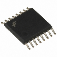
74LCX138MTCX Fairchild Semiconductor, 74LCX138MTCX Datasheet - Page 4

74LCX138MTCX
Manufacturer Part Number
74LCX138MTCX
Description
DECODER/DEMUX 1OF8 16-TSSOP
Manufacturer
Fairchild Semiconductor
Series
74LCXr
Type
Decoder/Demultiplexerr
Datasheet
1.74LCX138MTCX.pdf
(12 pages)
Specifications of 74LCX138MTCX
Circuit
1 x 3:8
Independent Circuits
1
Current - Output High, Low
24mA, 24mA
Voltage Supply Source
Single Supply
Voltage - Supply
2 V ~ 3.6 V
Operating Temperature
-40°C ~ 85°C
Mounting Type
Surface Mount
Package / Case
16-TSSOP
Logic Type
Decoder
No. Of Outputs
8
Supply Voltage Range
2V To 3.6V
Logic Case Style
TSSOP
No. Of Pins
16
Operating Temperature Range
-40°C To +85°C
Filter Terminals
SMD
Rohs Compliant
Yes
Family Type
LCX
Applications
Memory Chip Select Address Decoding
Lead Free Status / RoHS Status
Lead free / RoHS Compliant
Other names
74LCX138MTCXTR
Available stocks
Company
Part Number
Manufacturer
Quantity
Price
Part Number:
74LCX138MTCX
Manufacturer:
ON/安森美
Quantity:
20 000
www.fairchildsemi.com
V
V
V
V
I
I
I
V
V
V
I
I
I
I
I
T
V
V
V
I
T
I
OFF
CC
IK
OK
O
CC
GND
Absolute Maximum Ratings
Recommended Operating Conditions
OH
Note 3: The Absolute Maximum Ratings are those values beyond which the safety of the device cannot be guaranteed. The device should not be operated
at these limits. The parametric values defined in the Electrical Characteristics tables are not guaranteed at the Absolute Maximum Ratings. The “Recom-
mended Operating Conditions” table will define the conditions for actual device operation.
Note 4: I
Note 5: Unused inputs must be held HIGH or LOW. They may not float.
DC Electrical Characteristics
I
Symbol
Symbol
IH
IL
OH
OL
Symbol
STG
CC
CC
I
O
A
t/ V
CC
I
O
/I
OL
O
Absolute Maximum Rating must be observed.
HIGH Level Input Voltage
LOW Level Input Voltage
HIGH Level Output Voltage
LOW Level Output Voltage
Input Leakage Current
Power-Off Leakage Current
Quiescent Supply Current
Increase in I
Supply Voltage
DC Input Voltage
DC Output Voltage
DC Input Diode Current
DC Output Diode Current
DC Output Source/Sink Current
DC Supply Current per Supply Pin
DC Ground Current per Ground Pin
Storage Temperature
Supply Voltage
Input Voltage
Output Voltage
Output Current
Free-Air Operating Temperature
Input Edge Rate, V
CC
Parameter
per Input
Parameter
IN
0.8V to 2.0V, V
Parameter
I
I
I
I
I
I
I
I
I
I
0
V
V
3.6V
V
OH
OH
OH
OH
OH
OL
OL
OL
OL
OL
(Note 3)
I
I
IH
or V
= 8mA
CC
V
= -8 mA
V
I
100 A
12 mA
16 mA
24 mA
V
CC
O
100 A
12 mA
18 mA
24 mA
V
CC
0.5 to V
5.5V
I
or GND
3.0V
5.5V
0.5 to 7.0
0.5 to 7.0
65 to 150
5.5V
0.6V
Value
Conditions
100
100
50
50
50
50
CC
4
(Note 5)
0.5
HIGH or LOW State
V
V
V
Output in HIGH or LOW State (Note 4)
V
V
V
CC
CC
CC
I
O
O
Data Retention
GND
GND
V
3.0V to 3.6V
2.7V to 3.0V
2.3V to 2.7V
CC
Operating
2.3 to 2.7
2.7 to 3.6
2.3 to 2.7
2.7 to 3.6
2.3 to 3.6
2.3 to 3.6
2.3 to 3.6
2.3 to 3.6
2.3 to 3.6
2.3 to 3.6
V
2.3
2.7
3.0
3.0
2.3
2.7
3.0
3.0
(V)
0.0
CC
Conditions
V
T
CC
Min
A
2.0
1.5
0.0
0.0
40.0
0.0
Min
1.7
2.0
1.8
2.2
2.4
2.2
0.2
40 C to 85 C
Max
85.0
10.0
V
3.6
3.6
5.5
24.0
12.0
Max
0.55
10.0
10.0
500
8.0
0.7
0.8
0.2
0.6
0.4
0.4
10.0
CC
5.0
Units
Units
ns/V
Units
mA
mA
mA
mA
mA
mA
V
V
V
C
V
V
V
V
V
V
V
C
A
A
A
A


