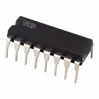
74HCT194N,652 NXP Semiconductors, 74HCT194N,652 Datasheet - Page 10

74HCT194N,652
Manufacturer Part Number
74HCT194N,652
Description
IC 4BIT BI UNIV SHIFT REG 16-DIP
Manufacturer
NXP Semiconductors
Series
74HCTr
Datasheet
1.74HC194DB112.pdf
(10 pages)
Specifications of 74HCT194N,652
Package / Case
16-DIP (0.300", 7.62mm)
Logic Type
Register, Bidirectional
Function
Universal
Output Type
Standard
Number Of Elements
1
Number Of Bits Per Element
4
Voltage - Supply
4.5 V ~ 5.5 V
Operating Temperature
-40°C ~ 125°C
Mounting Type
Through Hole
Counting Sequence
Serial/Parallel to Parallel
Number Of Circuits
1
Logic Family
HCT
Propagation Delay Time
15 ns
Supply Voltage (max)
5.5 V
Maximum Operating Temperature
+ 125 C
Minimum Operating Temperature
- 40 C
Mounting Style
SMD/SMT
Supply Voltage (min)
4.5 V
Lead Free Status / RoHS Status
Lead free / RoHS Compliant
Lead Free Status / RoHS Status
Lead free / RoHS Compliant, Lead free / RoHS Compliant
Other names
74HCT194N
74HCT194N
933670120652
74HCT194N
933670120652
Philips Semiconductors
AC WAVEFORMS
December 1990
4-bit bidirectional universal shift register
(1) HC : V
Fig.7
The shaded areas indicate when the input is permitted to
change for predictable output performance.
(1) HC : V
Fig.9
HCT: V
HCT: V
Waveforms showing the clock (CP) to
output (Q
pulse width, the output transition times and
the maximum clock frequency.
Waveforms showing the set-up and hold
times from the data inputs (D
D
M
M
M
M
SL
= 50%; V
= 50%; V
= 1.3 V; V
= 1.3 V; V
) to the clock (CP).
n
I
I
I
) propagation delays, the clock
I
= GND to V
= GND to V
= GND to 3 V.
= GND to 3 V.
CC
CC
.
.
n
, D
SR
and
10
PACKAGE OUTLINES
See
(1) HC : V
Fig.8
The shaded areas indicate when the input is permitted to
change for predictable output performance.
(1) HC : V
Fig.10 Waveforms showing the set-up and hold
“74HC/HCT/HCU/HCMOS Logic Package Outlines”
HCT: V
HCT: V
Waveforms showing the master reset (MR)
pulse width, the master reset to output (Q
propagation delays and the master reset to
clock (CP) removal time.
times from the mode control inputs (S
the clock input (CP).
M
M
M
M
= 50%; V
= 1.3 V; V
= 50%; V
= 1.3 V; V
I
I
I
I
= GND to V
= GND to V
= GND to 3 V.
= GND to 3 V.
CC
CC
.
.
74HC/HCT194
Product specification
n
) to
n
)
.


