MM74C221N Fairchild Semiconductor, MM74C221N Datasheet
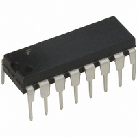
IC MULTIVIBRATOR MONO DUAL 16DIP

MM74C221N

Manufacturer Part Number
MM74C221N
Description
IC MULTIVIBRATOR MONO DUAL 16DIP
Manufacturer
Fairchild Semiconductor
Series
74Cr
Datasheet

Specifications of MM74C221N

Logic Type
Monostable
Independent Circuits
2
Schmitt Trigger Input
No
Propagation Delay
120ns
Current - Output High, Low
8mA, 8mA
Voltage - Supply
4.5 V ~ 15 V
Operating Temperature
-55°C ~ 125°C
Mounting Type
Through Hole
Package / Case
16-DIP (0.300", 7.62mm)
Lead Free Status / RoHS Status
Lead free / RoHS Compliant
Other names
74C221
74C221N

Available stocks

Company
Part Number
Manufacturer
Quantity
Price
Part Number:
MM74C221N
Quantity:
1
Part Number:
MM74C221N
Manufacturer:
NS
Quantity:
6 474
Part Number:
MM74C221N
Manufacturer:
NS/国半
Quantity:
20 000
© 1999 Fairchild Semiconductor Corporation
74MMC221N
MM74C221
Dual Monostable Multivibrator
General Description
The MM74C221 dual monostable multivibrator is a mono-
lithic complementary MOS integrated circuit. Each multivi-
brator features a negative-transition-triggered input and a
positive-transition-triggered input, either of which can be
used as an inhibit input, and a clear input.
Once fired, the output pulses are independent of further
transitions of the A and B inputs and are a function of the
external timing components C
width is stable over a wide range of temperature and V
Ordering Code:
Connection Diagrams
Order Number
Pin Assignments for DIP
Package Number
Timing Component
Top View
N16E
EXT
and R
16-Lead Plastic Dual-in-Line Package (PDIP), JEDEC MS-001, 0.300” Wide
EXT
DS005904.prf
. The pulse
CC
.
Pulse stability will be limited by the accuracy of external
timing components. The pulse width is approximately
defined by the relationship t
ther information and applications, see AN-138.
Features
Truth Table
H
L
Wide supply voltage range:
Guaranteed noise margin: 1.0V
High noise immunity: 0.45 V
Low power TTL compatibility: fan out of 2 driving 74L
LOW Level
Transition from LOW-to-HIGH
Transition from HIGH-to-LOW
HIGH Level
Package Description
Clear
H
L
X
X
H
Inputs
One LOW level pulse
One HIGH level pulse
A
X
X
L
H
W(OUT)
X Irrelevant
November 1987
Revised January 1999
CC
B
X
H
4.5V to 15V
L
X
(typ.)
C
EXT
www.fairchildsemi.com
Q
L
L
L
Outputs
R
EXT
. For fur-
H
H
H
Q

Related parts for MM74C221N

MM74C221N Summary of contents

Page 1

... Plastic Dual-in-Line Package (PDIP), JEDEC MS-001, 0.300” Wide Connection Diagrams Timing Component Pin Assignments for DIP Top View © 1999 Fairchild Semiconductor Corporation Pulse stability will be limited by the accuracy of external timing components. The pulse width is approximately defined by the relationship t ther information and applications, see AN-138. ...

Page 2

Absolute Maximum Ratings Voltage at Any Pin 0. Operating Temperature Range Storage Temperature Range Power Dissipation Dual-In-Line Small Outline Operating V Range CC DC Electrical Characteristics Max/min limits apply across temperature range, unless otherwise noted Symbol Parameter CMOS ...

Page 3

AC Electrical Characteristics pF, unless otherwise noted A L Symbol Parameter t Propagation Delay from Trigger Input ( Output Propagation Delay from Clear pd CL Input (CL) ...

Page 4

Typical Performance Characteristics 0% Point pulse width 5V 10V 15V,T 9 Percentage of units within 4 5V,90% of units CC ...

Page 5

Typical Performance Characteristics Switching Time Waveforms (Continued) 5 www.fairchildsemi.com ...

Page 6

Physical Dimensions inches (millimeters) unless otherwise noted 16-Lead Plastic Dual-In-Line Package (PDIP), JEDEC MS-001, 0.300” Wide LIFE SUPPORT POLICY FAIRCHILD’S PRODUCTS ARE NOT AUTHORIZED FOR USE AS CRITICAL COMPONENTS IN LIFE SUPPORT DEVICES OR SYSTEMS WITHOUT THE EXPRESS WRITTEN APPROVAL ...

Related keywords