MC10H209P ON Semiconductor, MC10H209P Datasheet
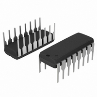
IC GATE OR/NOR DUAL 4-5 16-DIP

MC10H209P

Manufacturer Part Number
MC10H209P
Description
IC GATE OR/NOR DUAL 4-5 16-DIP
Manufacturer
ON Semiconductor
Series
10Hr
Datasheet

Specifications of MC10H209P

Logic Type
NOR/OR Gate
Number Of Circuits
2
Number Of Inputs
9 Input (4, 5)
Schmitt Trigger Input
No
Output Type
Differential
Operating Temperature
0°C ~ 75°C
Mounting Type
Through Hole
Package / Case
16-DIP (0.300", 7.62mm)
Lead Free Status / RoHS Status
Contains lead / RoHS non-compliant
Voltage - Supply
-
Current - Output High, Low
-

Available stocks

Company
Part Number
Manufacturer
Quantity
Price
Part Number:
MC10H209P
Manufacturer:
NS
Quantity:
3 942
Part Number:
MC10H209P
Manufacturer:
MOTOROLA/摩托罗拉
Quantity:
20 000
Part Number:
MC10H209PD
Manufacturer:
MOT
Quantity:
6 269
MC10H209
Dual 4−5−Input OR/NOR
Gate
Description
part is a functional/pinout duplication of the MECL III part MC1688.
Features
*For additional information on our Pb−Free strategy and soldering details, please
© Semiconductor Components Industries, LLC, 2006
February, 2006 − Rev. 7
download the ON Semiconductor Soldering and Mounting Techniques
Reference Manual, SOLDERRM/D.
The MC10H209 is a Dual 4−5−input OR/NOR gate. This MECL
Temperature Range)
Propagation Delay Average, 0.75 ns Typical
Power Dissipation 125 mW Typical
Improved Noise Margin 150 mV (Over Operating Voltage and
Voltage Compensated
MECL 10K™ Compatible
Pb−Free Packages are Available*
For PLCC pin assignment, see the Pin Conversion Tables on page 18
of the ON Semiconductor MECL Data Book (DL122/D).
Pin assignment is for Dual−in−Line Package.
A
A
V
10
12
13
11
V
OUT
OUT
4
5
6
7
9
CC1
A
A
A
A
EE
IN
IN
IN
IN
PIN ASSIGNMENT
LOGIC DIAGRAM
V
V
V
2
3
4
5
6
7
8
CC1
CC2
EE
1
= PIN 8
= PIN 1
= PIN 16
DIP
16
15
14
13
12
11
10
9
V
B
B
B
B
B
B
B
CC2
OUT
OUT
IN
IN
IN
IN
IN
3
2
14
15
1
See detailed ordering and shipping information in the package
dimensions section on page 3 of this data sheet.
16
20 1
*For additional marking information, refer to
CASE 620A
SOEIAJ−16
FN SUFFIX
Application Note AND8002/D.
CASE 648
CASE 966
CASE 775
1
P SUFFIX
L SUFFIX
PLLC−20
CDIP−16
PDIP−16
A
WL, L
YY, Y
WW, W = Work Week
G
ORDERING INFORMATION
http://onsemi.com
= Assembly Location
= Wafer Lot
= Year
= Pb−Free Package
16
MARKING DIAGRAMS*
1
Publication Order Number:
16
1
MC10H209L
AWLYYWW
AWLYYWW
MC10H209P
AWLYYWW
10H209G
ALYWG
10H209
1 20
MC10H209/D

Related parts for MC10H209P

MC10H209P Summary of contents

Page 1

... OUT http://onsemi.com MARKING DIAGRAMS* 16 MC10H209L AWLYYWW 1 CDIP−16 L SUFFIX CASE 620A 16 MC10H209P 16 AWLYYWW 1 1 PDIP−16 P SUFFIX CASE 648 10H209 ALYWG SOEIAJ−16 CASE 966 10H209G AWLYYWW PLLC−20 FN SUFFIX CASE 775 A = Assembly Location WL Wafer Lot YY Year WW Work Week G = Pb−Free Package *For additional marking information, refer to Application Note AND8002/D ...

Page 2

Table 1. MAXIMUM RATINGS Symbol V Power Supply ( Input Voltage ( Output Current − Continuous out − Surge T Operating Temperature Range A T Storage Temperature Range − Plastic ...

Page 3

... MC10H209FN MC10H209FNG MC10H209FNR2 MC10H209FNR2G MC10H209L MC10H209M MC10H209MEL MC10H209MELG MC10H209P †For information on tape and reel specifications, including part orientation and tape sizes, please refer to our Tape and Reel Packaging Specifications Brochure, BRD8011/D. Package PLLC−20 PLLC−20 (Pb−Free) PLLC−20 PLLC−20 (Pb− ...

Page 4

Y BRK −L− −M− 0.007 (0.180) Z 0.007 (0.180 −T− J VIEW S G1 0.010 (0.250) T L− NOTES: 1. DIMENSIONS AND TOLERANCING PER ANSI Y14.5M, ...

Page 5

VIEW 0.10 (0.004) 0.13 (0.005 0.25 (0.010) PACKAGE DIMENSIONS SOEIAJ−16 CASE 966−01 ISSUE ...

Page 6

... American Technical Support: 800−282−9855 Toll Free USA/Canada Japan: ON Semiconductor, Japan Customer Focus Center 2−9−1 Kamimeguro, Meguro−ku, Tokyo, Japan 153−0051 Phone: 81−3−5773−3850 http://onsemi.com 6 NOTES: 1. DIMENSIONING AND TOLERANCING PER ANSI Y14.5M, 1982. 2. CONTROLLING DIMENSION: INCH. ...

Related keywords