MC74LCX04DG ON Semiconductor, MC74LCX04DG Datasheet
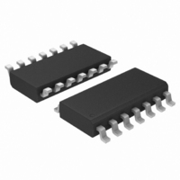
IC INVERTER HEX LV CMOS 14SOIC

MC74LCX04DG

Manufacturer Part Number
MC74LCX04DG
Description
IC INVERTER HEX LV CMOS 14SOIC
Manufacturer
ON Semiconductor
Series
74LCXr
Datasheet

Specifications of MC74LCX04DG

Logic Type
Inverter
Number Of Inputs
1
Number Of Circuits
6
Current - Output High, Low
24mA, 24mA
Voltage - Supply
2 V ~ 3.6 V
Operating Temperature
-40°C ~ 85°C
Mounting Type
Surface Mount
Package / Case
14-SOIC (3.9mm Width), 14-SOL
Logical Function
Inverter
Logic Family
LCX
Number Of Elements
6
High Level Output Current
-24mA
Low Level Output Current
24mA
Propagation Delay Time
6.2ns
Operating Supply Voltage (typ)
2.5/3.3V
Package Type
SOIC
Operating Temp Range
-55C to 125C
Pin Count
14
Quiescent Current
10uA
Technology
CMOS
Mounting
Surface Mount
Operating Temperature Classification
Military
Operating Supply Voltage (max)
5.5V
Operating Supply Voltage (min)
2V
Output Current
24mA
No. Of Inputs
1
Supply Voltage Range
2V To 3.6V
Logic Case Style
SOIC
No. Of Pins
14
Operating Temperature Range
-40°C To +85°C
Filter Terminals
SMD
Rohs Compliant
Yes
Family Type
LCX
Lead Free Status / RoHS Status
Lead free / RoHS Compliant
Other names
MC74LCX04DGOS
MC74LCX04
Low-Voltage CMOS Hex
Inverter
With 5 V−Tolerant Inputs
from a 2.0 to 5.5 V supply. High impedance TTL compatible inputs
significantly reduce current loading to input drivers while TTL
compatible outputs offer improved switching noise performance. A V
specification of 5.5 V allows MC74LCX04 inputs to be safely driven
from 5 V devices if V
Features
*For additional information on our Pb−Free strategy and soldering details, please
© Semiconductor Components Industries, LLC, 2009
December, 2009 − Rev. 5
download the ON Semiconductor Soldering and Mounting Techniques
Reference Manual, SOLDERRM/D.
The MC74LCX04 is a high performance hex inverter operating
Current drive capability is 24 mA at the outputs.
System Power Requirements
Designed for 2.0 V to 5.5 V V
5 V Tolerant Inputs − Interface Capability With 5 V TTL Logic
LVTTL Compatible
LVCMOS Compatible
24 mA Balanced Output Sink and Source Capability
Near Zero Static Supply Current (10 mA) Substantially Reduces
Latchup Performance Exceeds 500 mA
ESD Performance:
Pb−Free Packages are Available*
CC
Human Body Model >2000 V;
Machine Model >200 V
is less than 5.0 V.
CC
Operation
1
I
14
See detailed ordering and shipping information in the package
dimensions section on page 4 of this data sheet.
14
14
(Note: Microdot may be in either location)
1
1
1
ORDERING INFORMATION
A
WL, L
YY, Y
WW, W = Work Week
G or G
http://onsemi.com
CASE 751A
SOEIAJ−14
D SUFFIX
CASE 948G
SOIC−14
DT SUFFIX
CASE 965
TSSOP−14
M SUFFIX
= Assembly Location
= Wafer Lot
= Year
= Pb−Free Package
Publication Order Number:
14
1
14
1
DIAGRAMS
14
1
MARKING
MC74LCX04/D
AWLYWW
LCX04G
74LCX04
ALYWG
ALYWG
LCX
04
G

Related parts for MC74LCX04DG

MC74LCX04DG Summary of contents

Page 1

... Human Body Model >2000 V; Machine Model >200 V • Pb−Free Packages are Available* *For additional information on our Pb−Free strategy and soldering details, please download the ON Semiconductor Soldering and Mounting Techniques Reference Manual, SOLDERRM/D. © Semiconductor Components Industries, LLC, 2009 December, 2009 − Rev. 5 http://onsemi.com I SOIC− ...

Page 2

GND Figure 1. Pinout: 14−Lead (Top View) PIN NAMES Pins Function An Data Inputs On Outputs MAXIMUM RATINGS ...

Page 3

RECOMMENDED OPERATING CONDITIONS Symbol V Supply Voltage CC V Input Voltage I V Output Voltage O I HIGH Level Output Current OH I LOW Level Output Current OL T Operating Free−Air Temperature A Dt/DV Input Transition Rise or Fall Rate, ...

Page 4

... Input Capacitance IN C Output Capacitance OUT C Power Dissipation Capacitance PD ORDERING INFORMATION Device MC74LCX04DG MC74LCX04DR2 MC74LCX04DR2G MC74LCX04DT MC74LCX04DTG MC74LCX04DTR2 MC74LCX04DTR2G MC74LCX04MELG †For information on tape and reel specifications, including part orientation and tape sizes, please refer to our Tape and Reel Packaging Specifications Brochure, BRD8011/D. ...

Page 5

Vmi An t PHL Vmo On WAVEFORM 1 − PROPAGATION DELAYS 2.5 ns, 10 MHz 3 0.3 V Symbol Vmi 1.5 V Vmo 1.5 V Figure ...

Page 6

G −T− SEATING 14 PL PLANE 0.25 (0.010 PACKAGE DIMENSIONS SOIC−14 D SUFFIX CASE 751A−03 ISSUE 0.25 (0.010 ...

Page 7

K 14X REF 0.10 (0.004) 0.15 (0.006 L PIN 1 IDENT. 1 0.15 (0.006 −V− C 0.10 (0.004) −T− G SEATING D PLANE 14X 0.36 PACKAGE DIMENSIONS TSSOP−14 DT SUFFIX ...

Page 8

... Opportunity/Affirmative Action Employer. This literature is subject to all applicable copyright laws and is not for resale in any manner. PUBLICATION ORDERING INFORMATION LITERATURE FULFILLMENT: Literature Distribution Center for ON Semiconductor P.O. Box 5163, Denver, Colorado 80217 USA Phone: 303−675−2175 or 800−344−3860 Toll Free USA/Canada Fax: 303− ...

Related keywords