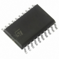
74LVX374MTR STMicroelectronics, 74LVX374MTR Datasheet

74LVX374MTR
Specifications of 74LVX374MTR
Available stocks
Related parts for 74LVX374MTR
74LVX374MTR Summary of contents
Page 1
... CMOS low power consumption. All inputs and outputs are equipped with protection circuits against static discharge, giving them 2KV ESD immunity and transient excess voltage. 74LVX374 SOP TSSOP PACKAGE T & R SOP 74LVX374MTR TSSOP 74LVX374TTR Rev. 3 1/13 ...
Page 2
Figure 2: Input Equivalent Circuit Table 3: Truth Table Don’t Care Z : High Impedance Figure 3: Logic Diagram This logic diagram has not be used to estimate propagation delays 2/13 Table ...
Page 3
Table 4: Absolute Maximum Ratings Symbol V Supply Voltage Input Voltage Output Voltage Input Diode Current Output Diode Current Output Current ...
Page 4
Table 7: Dynamic Switching Characteristics Symbol Parameter V Dynamic Low OLP Voltage Quiet V OLV Output (note 1, 2) Dynamic High V Voltage Input IHD (note 1, 3) Dynamic Low V Voltage Input ILD (note Worst ...
Page 5
Table 9: Capacitive Characteristics Symbol Parameter C Input Capacitance IN C Output OUT Capacitance C Power Dissipation PD Capacitance (note defined as the value of the IC’s internal equivalent capacitance which is calculated from the operating ...
Page 6
Figure 5: Waveform - Propagation Delays Setup And Hold Times (f=1MHz; 50% duty cycle) Figure 6: Waveform - Output Enable And Disable Times (f=1MHz; 50% duty cycle) 6/13 ...
Page 7
Figure 7: Waveform - Minimum Pulse Width (f=1MHz; 50% duty cycle) 74LVX374 7/13 ...
Page 8
DIM. MIN. A 2.35 A1 0.1 B 0.33 C 0.23 D 12. 10.00 h 0.25 L 0.4 k 0° ddd 8/13 SO-20 MECHANICAL DATA mm. TYP MAX. 2.65 0.30 0.51 0.32 13.00 7.6 1.27 10.65 ...
Page 9
TSSOP20 MECHANICAL DATA DIM. MIN 0.05 A2 0.8 b 0.19 c 0.09 D 6.4 E 6 0˚ PIN 1 IDENTIFICATION 1 mm. TYP MAX. 1.2 0.15 1 1.05 ...
Page 10
DIM. MIN 12 10.8 Bo 13.2 Ko 3.1 Po 3.9 P 11.9 10/13 Tape & Reel SO-20 MECHANICAL DATA mm. TYP MAX. 330 13.2 30.4 11 13.4 3.3 4.1 12.1 inch ...
Page 11
Tape & Reel TSSOP20 MECHANICAL DATA DIM. MIN 12 6.8 Bo 6.9 Ko 1.7 Po 3.9 P 11.9 mm. TYP MAX. 330 13.2 0.504 0.795 2.362 22.4 7 0.268 7.1 0.272 1.9 ...
Page 12
Table 10: Revision History Date Revision 27-Aug-2004 3 12/13 Description of Changes Ordering Codes Revision - pag. 1. ...
Page 13
... No license is granted by implication or otherwise under any patent or patent rights of STMicroelectronics. Specifications mentioned in this publication are subject to change without notice. This publication supersedes and replaces all information previously supplied. STMicroelectronics products are not authorized for use as critical components in life support devices or systems without express written approval of STMicroelectronics ...


