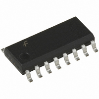
MM74HC175M Fairchild Semiconductor, MM74HC175M Datasheet - Page 3

MM74HC175M
Manufacturer Part Number
MM74HC175M
Description
IC FLIP FLOP QUAD D 16-SOIC
Manufacturer
Fairchild Semiconductor
Series
74HCr
Type
D-Type Busr
Datasheet
1.MM74HC175MX.pdf
(7 pages)
Specifications of MM74HC175M
Function
Master Reset
Output Type
Differential
Number Of Elements
1
Number Of Bits Per Element
4
Frequency - Clock
60MHz
Delay Time - Propagation
15ns
Trigger Type
Positive Edge
Current - Output High, Low
5.2mA, 5.2mA
Voltage - Supply
2 V ~ 6 V
Operating Temperature
-40°C ~ 85°C
Mounting Type
Surface Mount
Package / Case
16-SOIC (3.9mm Width)
Flip-flop Type
D
Propagation Delay
13ns
Frequency
60MHz
Output Current
5.2mA
Ic Output Type
Differential / Complementary
Supply Voltage Range
2V To 6V
Rohs Compliant
Yes
Lead Free Status / RoHS Status
Lead free / RoHS Compliant
Available stocks
Company
Part Number
Manufacturer
Quantity
Price
Part Number:
MM74HC175M
Manufacturer:
FAIRCHILD/仙童
Quantity:
20 000
Company:
Part Number:
MM74HC175MTCX
Manufacturer:
Fairchild Semiconductor
Quantity:
135
Company:
Part Number:
MM74HC175MTCX
Manufacturer:
VISHAY
Quantity:
23 320
Company:
Part Number:
MM74HC175MX
Manufacturer:
FSC
Quantity:
2 495
Company:
Part Number:
MM74HC175MX
Manufacturer:
FSC
Quantity:
4 157
Part Number:
MM74HC175MX
Manufacturer:
FSC
Quantity:
20 000
V
V
V
V
I
I
IN
CC
Symbol
Absolute Maximum Ratings
(Note 2)
DC Electrical Characteristics
Note 4: For a power supply of 5V 10% the worst case output voltages (V
designing with this supply. Worst case V
rent (I
IH
IL
OH
OL
Supply Voltage (V
DC Input Voltage (V
DC Output Voltage (V
Clamp Diode Current (I
DC Output Current, per pin (I
DC V
Storage Temperature Range (T
Power Dissipation (P
Lead Temperature (T
(Note 3)
S.O. Package only
(Soldering 10 seconds)
IN
CC
, I
CC
Minimum HIGH Level
Input Voltage
Maximum LOW Level
Input Voltage
Minimum HIGH Level
Output Voltage
Maximum LOW Level
Output Voltage
Maximum Input
Current
Maximum Quiescent
Supply Current
or GND Current, per pin (I
, and I
OZ
Parameter
) occur for CMOS at the higher voltage and so the 6.0V values should be used.
CC
IN
)
D
L
)
OUT
)
)
IK
, I
)
OK
OUT
)
IH
STG
)
and V
V
|I
V
|I
|I
V
|I
V
|I
|I
V
V
I
OUT
CC
)
OUT
OUT
OUT
OUT
OUT
OUT
IN
IN
IN
IN
IN
IN
)
IL
|
|
|
|
|
|
V
V
V
V
V
V
occur at V
Conditions
0 A
IH
IH
IH
IH
CC
CC
20 A
4.0 mA
5.2 mA
20 A
4.0 mA
5.2 mA
or V
or V
or V
or V
1.5 to V
0.5 to V
or GND
or GND
65 C to 150 C
IL
IL
IL
IL
(Note 1)
0.5 to 7.0V
CC
(Note 4)
CC
CC
600 mW
500 mW
5.5V and 4.5V respectively. (The V
20 mA
25 mA
50 mA
260 C
1.5V
0.5V
2.0V
4.5V
6.0V
2.0V
4.5V
6.0V
2.0V
4.5V
6.0V
4.5V
6.0V
2.0V
4.5V
6.0V
4.5V
6.0V
6.0V
6.0V
V
OH
CC
, and V
3
Supply Voltage (V
DC Input or Output Voltage
Operating Temperature Range (T
Input Rise or Fall Times
Recommended Operating
Conditions
Note 1: Absolute Maximum Ratings are those values beyond which dam-
age to the device may occur.
Note 2: Unless otherwise specified all voltages are referenced to ground.
Note 3: Power Dissipation temperature derating — plastic “N” package:
12 mW/ C from 65 C to 85 C.
(V
(t
r
OL
, t
IN
Typ
2.0
4.5
6.0
4.2
5.7
0.2
0.2
) occur for HC at 4.5V. Thus the 4.5V values should be used when
f
,V
) V
0
0
0
T
OUT
A
V
V
CC
CC
CC
25 C
)
3.15
1.35
3.98
5.48
0.26
0.26
1.5
4.2
0.5
1.8
1.9
4.4
5.9
0.1
0.1
0.1
2.0V
IH
0.1
8
4.5V
6.0V
value at 5.5V is 3.85V.) The worst case leakage cur-
CC
)
T
A
Guaranteed Limits
40 to 85 C T
3.15
1.35
3.84
5.34
0.33
0.33
1.5
4.2
0.5
1.8
1.9
4.4
5.9
0.1
0.1
0.1
80
1.0
A
)
Min
2
0
40
A
www.fairchildsemi.com
55 to 125 C
3.15
1.35
1000
160
1.5
Max
4.2
0.5
1.8
1.9
4.4
5.9
3.7
5.2
0.1
0.1
0.1
0.4
0.4
V
500
400
1.0
6
85
CC
Units
ns
ns
ns
V
V
C
Units
V
V
V
V
V
V
V
V
V
V
V
V
V
V
V
V
A
A


