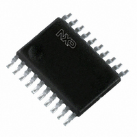
74HC273PW,118 NXP Semiconductors, 74HC273PW,118 Datasheet - Page 11

74HC273PW,118
Manufacturer Part Number
74HC273PW,118
Description
IC OCTAL D F-F POS-EDGE 20-TSSOP
Manufacturer
NXP Semiconductors
Series
74HCr
Type
D-Type Busr
Datasheet
1.74HC273PW118.pdf
(26 pages)
Specifications of 74HC273PW,118
Output Type
Non-Inverted
Package / Case
20-TSSOP
Function
Master Reset
Number Of Elements
1
Number Of Bits Per Element
8
Frequency - Clock
122MHz
Delay Time - Propagation
13ns
Trigger Type
Positive Edge
Current - Output High, Low
5.2mA, 5.2mA
Voltage - Supply
2 V ~ 6 V
Operating Temperature
-40°C ~ 125°C
Mounting Type
Surface Mount
Number Of Circuits
1
Logic Family
HC
Logic Type
D-Type Edge Triggered Flip-Flop
Polarity
Non-Inverting
Input Type
Single-Ended
Propagation Delay Time
15 ns at 5 V
High Level Output Current
- 5.2 mA
Low Level Output Current
5.2 mA
Supply Voltage (max)
6 V
Maximum Operating Temperature
+ 125 C
Mounting Style
SMD/SMT
Minimum Operating Temperature
- 40 C
Supply Voltage (min)
2 V
Lead Free Status / RoHS Status
Lead free / RoHS Compliant
Lead Free Status / RoHS Status
Lead free / RoHS Compliant, Lead free / RoHS Compliant
Other names
568-4477-2
74HC273PW-T
74HC273PW-T
935185830118
74HC273PW-T
74HC273PW-T
935185830118
Available stocks
Company
Part Number
Manufacturer
Quantity
Price
Company:
Part Number:
74HC273PW,118
Manufacturer:
NXP Semiconductors
Quantity:
2 000
Philips Semiconductors
Table 8:
At recommended operating conditions; voltages are referenced to GND (ground = 0 V).
11. Dynamic characteristics
Table 9:
Voltages are referenced to GND (ground = 0 V); t
Figure
74HC_HCT273_3
Product data sheet
Symbol
I
I
Symbol Parameter
T
t
t
t
t
t
t
OZ
CC
PHL
PLH
PHL
THL
TLH
W
I
amb
CC
,
,
= 25 C
10.
propagation delay CP to Qn
HIGH-to-LOW propagation delay
MR to Qn
output transition time
pulse width
Static characteristics 74HCT273
Dynamic characteristics 74HC273
clock HIGH or LOW
master reset LOW
Parameter
OFF-state output current
quiescent supply current
additional quiescent supply
current
pin MR
pin CP
pin Dn
Conditions
see
see
see
see
see
…continued
V
V
V
V
V
V
V
V
V
V
V
V
V
V
V
V
V
Conditions
V
V
other inputs at V
V
V
V
V
I
O
r
CC
CC
CC
CC
CC
CC
CC
CC
CC
CC
CC
CC
CC
CC
CC
CC
CC
Rev. 03 — 24 January 2006
I
O
I
CC
I
CC
Figure 7
Figure 8
Figure 7
Figure 7
Figure 8
= t
= V
= V
= V
= 0 A
= V
= 2.0 V
= 4.5 V
= 5 V; C
= 6.0 V
= 2.0 V
= 4.5 V
= 5 V; C
= 6.0 V
= 2.0 V
= 4.5 V
= 6.0 V
= 2.0 V
= 4.5 V
= 6.0 V
= 2.0 V
= 4.5 V
= 6.0 V
= 5.5 V
or GND; V
f
= 6 ns; C
IH
CC
CC
CC
or V
or GND; I
or GND per input pin;
2.1 V; other inputs at
L
L
Octal D-type flip-flop with reset; positive-edge trigger
IL
; V
= 15 pF
= 15 pF
L
CC
CC
= 50 pF unless otherwise specified; for test circuit see
CC
= 4.5 V to 5.5 V;
O
or GND; I
= 5.5 V;
= 0 A;
74HC273; 74HCT273
O
= 0 A
Min
-
-
-
-
-
-
-
-
-
-
-
80
16
14
60
12
10
© Koninklijke Philips Electronics N.V. 2006. All rights reserved.
Min
-
-
-
-
-
Typ
41
15
15
13
44
16
15
14
19
7
6
14
5
4
17
6
5
Typ
-
-
-
-
-
Max
150
30
-
26
150
30
-
26
75
15
13
-
-
-
-
-
-
Max
160
490
857.5
73.5
10
11 of 26
Unit
ns
ns
ns
ns
ns
ns
ns
ns
ns
ns
ns
ns
ns
ns
ns
ns
ns
Unit
A
A
A
A
A


