IDT72605L20J IDT, Integrated Device Technology Inc, IDT72605L20J Datasheet - Page 5
IDT72605L20J
Manufacturer Part Number
IDT72605L20J
Description
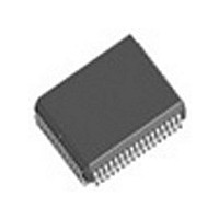
IC FIFO BI SYNC 256X18 68-PLCC
Manufacturer
IDT, Integrated Device Technology Inc
Series
7200r
Datasheet
1.IDT72605L50PF8.pdf
(17 pages)
Specifications of IDT72605L20J
Function
Synchronous
Memory Size
9.2K (512 x 18)
Data Rate
50MHz
Access Time
20ns
Voltage - Supply
4.5 V ~ 5.5 V
Operating Temperature
0°C ~ 70°C
Mounting Type
Surface Mount
Package / Case
68-PLCC
Configuration
Dual
Density
9Kb
Access Time (max)
10ns
Word Size
18b
Organization
256x18x2
Sync/async
Synchronous
Expandable
No
Bus Direction
Bi-Directional
Package Type
PLCC
Clock Freq (max)
50MHz
Operating Supply Voltage (typ)
5V
Operating Supply Voltage (min)
4.5V
Operating Supply Voltage (max)
5.5V
Supply Current
230mA
Operating Temp Range
-40C to 85C
Operating Temperature Classification
Industrial
Mounting
Surface Mount
Pin Count
68
Lead Free Status / RoHS Status
Contains lead / RoHS non-compliant
Other names
72605L20J
Available stocks
Company
Part Number
Manufacturer
Quantity
Price
Company:

Part Number:
IDT72605L20J
Manufacturer:
IDT, Integrated Device Technology Inc
Quantity:
10 000
Company:
Part Number:
IDT72605L20J8
Manufacturer:
IDT, Integrated Device Technology Inc
Quantity:
10 000


AC TEST CONDITIONS
AC ELECTRICAL CHARACTERISTICS
(Industrial: V
NOTES:
1. Control signals refer to CS
2. Minimum values are guaranteed by design.
IDT72605/72615 CMOS SYNCBiFIFO™
256 x 18x 2 and 512 x 18 x 2
Symbol
f
t
t
t
t
t
t
t
t
t
t
t
t
t
t
t
t
t
t
t
t
t
CLK
CLK
CLKH
CLKL
RS
RSS
RSR
A
CS
CH
DS
DH
RSF
OE
OLZ
OHZ
FF
EF
PAE
PAF
SKEW1
SKEW2
In Pulse Levels
Input Rise/Fall Times
Input Timing Reference Levels
Output Reference Levels
Output Load
Clock frequency
Clock cycle time
Clock HIGH time
Clock LOW time
Reset pulse width
Reset setup time
Reset recovery time
Reset to flags in initial state
Data access time
Control signal setup time
Control signal hold time
Data setup time
Data hold time
Output Enable LOW to output data valid
Output Enable LOW to data bus at Low-Z
Output Enable HIGH to data bus at High-Z
Clock to Full Flag time
Clock to Empty Flag time
Clock to Programmable
Almost-Empty Flag time
Clock to Programmable
Almost-Full Flag time
Skew between CLK
for Empty/Full Flags
Skew between CLK
for Programmable Flags
CC
= 5V ± 10%, T
Parameter
A
, R/W
(2)
A
A
A
& CLK
& CLK
(1)
(2)
A
= -40°C to +85°C)
(1)
, EN
A
B
B
, A
2
, A
1
, A
(2)
(2)
0
, R/W
(2)
B
GND to 3.0V
See Figure 2
Min.
IDT72615L20
IDT72605L20
, EN
—
20
20
12
12
—
—
—
—
10
17
—
8
8
3
6
1
6
1
3
0
3
1.5V
1.5V
3ns
B
.
Max.
50
—
—
—
—
—
—
27
10
—
—
—
—
10
—
10
10
10
12
12
—
—
Min.
IDT72615L25
IDT72605L25
—
25
10
10
25
15
15
—
—
—
—
—
12
19
3
6
1
6
1
3
0
3
5
Max.
Industrial
40
—
—
—
—
—
—
28
15
—
—
—
—
13
—
13
15
15
15
15
—
—
Min.
IDT72615L35
IDT72605L35
—
35
14
14
35
21
21
—
—
—
—
17
25
—
3
8
1
8
1
3
0
3
D.U.T.
Max.
28
—
—
—
—
—
—
35
21
—
—
—
—
20
—
20
21
21
21
21
—
—
* Includes jig and scope capacitances.
Figure 2. Output Load
680Ω
Min.
or equivalent circuit
IDT72615L50
IDT72605L50
—
50
20
20
50
30
30
—
10
10
—
—
—
—
20
34
3
1
1
3
0
3
INDUSTRIAL TEMPERATURE RANGE
Max.
20
—
—
—
—
—
—
50
25
—
—
—
—
28
—
28
30
30
30
30
—
—
MHz
Unit
+5V
ns
ns
ns
ns
ns
ns
ns
ns
ns
ns
ns
ns
ns
ns
ns
ns
ns
ns
ns
ns
ns
30pF*
1.1KΩ
4,5,6,7,12,13,14,15
4,5,6,7,12,13,14,15
2704 drw 04
4,5,6,7,8,9,10,11,
Timing Figures
4,5,6,7,10,11,12,
4,5,6,7,8,9,10,11
4, 7,12,13,14,15
5,7,8,9,10,11
4,6,8,9,10,11
5,7,8,9,10,11
5,7,8,9,10,11
5,7,8,9,10,11
12, 13,14,15
13, 14,15
5,7,10,11
4,6,10,11
4,5,6,7
12,14
13,15
4,6
—
3
3
3
3
Related parts for IDT72605L20J
Image
Part Number
Description
Manufacturer
Datasheet
Request
R

Part Number:
Description:
TRANSLATION DEVICE DPI 80-PQFP
Manufacturer:
IDT, Integrated Device Technology Inc
Datasheet:
Part Number:
Description:
IDT PART
Manufacturer:
IDT, Integrated Device Technology Inc
Datasheet:
Part Number:
Description:
IC LIU T1/E1/J1 OCTAL 256PBGA
Manufacturer:
IDT, Integrated Device Technology Inc
Datasheet:

Part Number:
Description:
IC FREQ TIMING GENERATOR 28TSSOP
Manufacturer:
IDT, Integrated Device Technology Inc
Datasheet:
Part Number:
Description:
IC CLK DVR PLL 1:10 40VFQFPN
Manufacturer:
IDT, Integrated Device Technology Inc
Datasheet:
Part Number:
Description:
IC CLK FANOUT BUFFER 1:18 32LQFP
Manufacturer:
IDT, Integrated Device Technology Inc
Datasheet:
Part Number:
Description:
IC CLK FANOUT BUFFER 1:18 32LQFP
Manufacturer:
IDT, Integrated Device Technology Inc
Datasheet:
Part Number:
Description:
IC CK505 VREG/RES 56TSSOP
Manufacturer:
IDT, Integrated Device Technology Inc
Datasheet:

Part Number:
Description:
IC SDRAM CLK DVR 1:10 48-TSSOP
Manufacturer:
IDT, Integrated Device Technology Inc
Datasheet:

Part Number:
Description:
IC CLK DVR PLL 1:10 48TSSOP
Manufacturer:
IDT, Integrated Device Technology Inc
Datasheet:
Part Number:
Description:
IC FLEXPC CLK PROGR P4 56-TSSOP
Manufacturer:
IDT, Integrated Device Technology Inc
Datasheet:
Part Number:
Description:
IC FLEXPC CLK PROGR P4 56-TSSOP
Manufacturer:
IDT, Integrated Device Technology Inc
Datasheet:
Part Number:
Description:
IC FLEXPC CLK PROGR P4 56-SSOP
Manufacturer:
IDT, Integrated Device Technology Inc
Datasheet:

Part Number:
Description:
IC PLL CLK DRIVER 2.5V 28-TSSOP
Manufacturer:
IDT, Integrated Device Technology Inc
Datasheet:
Part Number:
Description:
IC CLOCK DRIVER 2.5V 24-TSSOP
Manufacturer:
IDT, Integrated Device Technology Inc
Datasheet: