MC14024BDG ON Semiconductor, MC14024BDG Datasheet
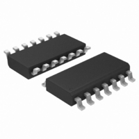
IC COUNTER RIPPLE 7STAGE 14SOIC

MC14024BDG

Manufacturer Part Number
MC14024BDG
Description
IC COUNTER RIPPLE 7STAGE 14SOIC
Manufacturer
ON Semiconductor
Series
4000Br
Datasheet

Specifications of MC14024BDG

Logic Type
Binary Counter
Direction
Up
Number Of Elements
1
Number Of Bits Per Element
7
Reset
Asynchronous
Count Rate
12MHz
Trigger Type
Positive, Negative
Voltage - Supply
3 V ~ 18 V
Operating Temperature
-55°C ~ 125°C
Mounting Type
Surface Mount
Package / Case
14-SOIC (3.9mm Width), 14-SOL
Lead Free Status / RoHS Status
Lead free / RoHS Compliant
Timing
-
Other names
MC14024BDGOS
MC14024B
7−Stage Ripple Counter
delays and high maximum clock rates. The Reset input has standard
noise immunity, however the Clock input has increased noise
immunity due to Hysteresis. The output of each counter stage is
buffered.
Features
Stresses exceeding Maximum Ratings may damage the device. Maximum
Ratings are stress ratings only. Functional operation above the Recommended
Operating Conditions is not implied. Extended exposure to stresses above the
Recommended Operating Conditions may affect device reliability.
1. Temperature Derating:
static voltages or electric fields. However, precautions must be taken to avoid
applications of any voltage higher than maximum rated voltages to this
high−impedance circuit. For proper operation, V
to the range V
either V
MAXIMUM RATINGS
© Semiconductor Components Industries, LLC, 2006
October, 2006 − Rev. 7
Symbol
V
I
The MC14024B is a 7−stage ripple counter with short propagation
in
This device contains protection circuitry to guard against damage due to high
Unused inputs must always be tied to an appropriate logic voltage level (e.g.,
Schottky TTL Load Over the Rated Temperature Range
in
Diode Protection on All Inputs
Output Transitions Occur on the Falling Edge of the Clock Pulse
Supply Voltage Range = 3.0 Vdc to 18 Vdc
Capable of Driving Two Low−power TTL Loads or One Low−power
Pin−for−Pin Replacement for CD4024B
Pb−Free Packages are Available
V
T
Plastic “P and D/DW” Packages: – 7.0 mW/_C From 65_C To 125_C
P
, V
, I
T
T
stg
DD
A
D
L
out
out
SS
or V
DC Supply Voltage Range
Input or Output Voltage Range
Input or Output Current
Power Dissipation, per Package
Ambient Temperature Range
Storage Temperature Range
Lead Temperature
SS
DD
(DC or Transient)
(DC or Transient) per Pin
(Note 1)
(8−Second Soldering)
v (V
). Unused outputs must be left open.
in
Parameter
or V
(Voltages Referenced to V
out
) v V
DD
.
in
and V
−0.5 to V
SS
−0.5 to +18.0
−55 to +125
−65 to +150
out
)
Value
± 10
500
260
should be constrained
DD
+ 0.5
1
Unit
mW
mA
°C
°C
°C
V
V
See detailed ordering and shipping information in the package
dimensions section on page 2 of this data sheet.
A
WL, L
YY, Y
WW, W
G
ORDERING INFORMATION
http://onsemi.com
CASE 751A
SOEIAJ−14
CASE 646
CASE 965
= Assembly Location
= Wafer Lot
= Year
= Work Week
= Pb−Free Package
P SUFFIX
D SUFFIX
F SUFFIX
PDIP−14
SOIC−14
Publication Order Number:
14
1
14
14
1
1
MC14024BCP
DIAGRAMS
AWLYYWWG
MARKING
MC14024B
AWLYWW
MC14024B/D
ALYWG
14024BG

Related parts for MC14024BDG

MC14024BDG Summary of contents

Page 1

MC14024B 7−Stage Ripple Counter The MC14024B is a 7−stage ripple counter with short propagation delays and high maximum clock rates. The Reset input has standard noise immunity, however the Clock input has increased noise immunity due to Hysteresis. The output ...

Page 2

... PIN PIN CONNECTION ORDERING INFORMATION Device MC14024BCP MC14024BCPG MC14024BD MC14024BDG MC14024BDR2 MC14024BDR2G MC14024BFEL MC14024BFELG †For information on tape and reel specifications, including part orientation and tape sizes, please refer to our Tape and Reel Packaging Specifications Brochure, BRD8011/D. TRUTH TABLE Clock Reset State ...

Page 3

ELECTRICAL CHARACTERISTICS Î Î Î Î Î ...

Page 4

SWITCHING CHARACTERISTICS (Note 5) Î Î Î ...

Page 5

out EXTERNAL V POWER SS COUNT SUPPLY LOGIC 1" LEVEL. Figure 1. Typical Output Source Characteristics Test Circuit 500 mF PULSE GENERATOR ...

Page 6

Figure 4. Functional Waveforms http://onsemi.com 6 ...

Page 7

−T− SEATING PLANE 0.13 (0.005) PACKAGE DIMENSIONS PDIP−14 CASE 646−06 ISSUE http://onsemi.com 7 NOTES: 1. DIMENSIONING AND TOLERANCING PER ANSI ...

Page 8

... G −T− SEATING 14 PL PLANE 0.25 (0.010 14X 0.58 *For additional information on our Pb−Free strategy and soldering details, please download the ON Semiconductor Soldering and Mounting Techniques Reference Manual, SOLDERRM/D. PACKAGE DIMENSIONS SOIC−14 CASE 751A−03 ISSUE 0.25 (0.010 ...

Page 9

... Opportunity/Affirmative Action Employer. This literature is subject to all applicable copyright laws and is not for resale in any manner. PUBLICATION ORDERING INFORMATION LITERATURE FULFILLMENT: Literature Distribution Center for ON Semiconductor P.O. Box 5163, Denver, Colorado 80217 USA Phone: 303−675−2175 or 800−344−3860 Toll Free USA/Canada Fax: 303− ...

Related keywords