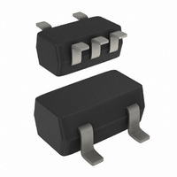
74LVC1G125GW,125 NXP Semiconductors, 74LVC1G125GW,125 Datasheet - Page 8

74LVC1G125GW,125
Manufacturer Part Number
74LVC1G125GW,125
Description
IC BUFF DVR TRI-ST N-INV 5TSSOP
Manufacturer
NXP Semiconductors
Series
74LVCr
Datasheet
1.74LVC1G125GV125.pdf
(19 pages)
Specifications of 74LVC1G125GW,125
Logic Type
Buffer/Line Driver, Non-Inverting
Package / Case
SC-70-5, SC-88A, SOT-323-5, SOT-353, 5-TSSOP
Number Of Elements
1
Number Of Bits Per Element
1
Current - Output High, Low
32mA, 32mA
Voltage - Supply
2 V ~ 5.5 V
Operating Temperature
-40°C ~ 125°C
Mounting Type
Surface Mount
Logic Family
74LVC
Number Of Channels Per Chip
1
Polarity
Non-Inverting
Supply Voltage (max)
5.5 V
Supply Voltage (min)
1.65 V
Maximum Operating Temperature
125 C
Mounting Style
SMD/SMT
High Level Output Current
- 32 mA
Input Bias Current (max)
200 uA
Low Level Output Current
32 mA
Maximum Power Dissipation
250 mW
Minimum Operating Temperature
- 40 C
Number Of Lines (input / Output)
2 / 1
Output Type
3-State
Propagation Delay Time
5.5 ns
Logical Function
Buffer/Line Driver
Number Of Elements
1
Number Of Channels
1
Number Of Inputs
1
Number Of Outputs
1
Operating Supply Voltage (typ)
1.8/2.5/3.3/5V
Package Type
TSSOP
Operating Supply Voltage (max)
5.5V
Operating Supply Voltage (min)
1.65V
Quiescent Current
200uA
Technology
CMOS
Pin Count
5
Mounting
Surface Mount
Operating Temp Range
-40C to 125C
Operating Temperature Classification
Automotive
Lead Free Status / RoHS Status
Lead free / RoHS Compliant
Lead Free Status / RoHS Status
Lead free / RoHS Compliant, Lead free / RoHS Compliant
Other names
568-3005-2
935268720125
935268720125
Available stocks
Company
Part Number
Manufacturer
Quantity
Price
Company:
Part Number:
74LVC1G125GW,125
Manufacturer:
NXP Semiconductors
Quantity:
4 300
NXP Semiconductors
12. Waveforms
Table 9.
74LVC1G125
Product data sheet
Supply voltage
V
1.65 V to 1.95 V
2.3 V to 2.7 V
2.7 V
3.0 V to 3.6 V
4.5 V to 5.5 V
Fig 7.
Fig 8.
CC
Measurement points are given in
V
Input A to output Y propagation delay times
Measurement points are given in
V
3-state enable and disable times
OL
OL
Measurement points
and V
and V
OH
OH
are typical output voltage levels that occur with the output load.
are typical output voltage levels that occur with the output load.
HIGH-to-OFF
OFF-to-HIGH
LOW-to-OFF
OFF-to-LOW
output
OE input
output
Y output
A input
Input
V
0.5V
0.5V
1.5 V
1.5 V
0.5V
M
GND
GND
V
V
Table
V
Table
OH
CC
OL
V
All information provided in this document is subject to legal disclaimers.
CC
CC
CC
I
GND
9.
9.
V
V
OH
OL
V
I
Rev. 9 — 29 December 2010
V
M
enabled
outputs
t
PLZ
t
PHZ
V
M
Output
V
0.5V
0.5V
1.5 V
1.5 V
0.5V
V
M
M
V
X
t
PHL
V
CC
CC
CC
Y
disabled
outputs
t
PZL
t
PZH
mnb153
V
V
V
V
V
V
t
X
OL
OL
OL
OL
OL
PLH
V
+ 0.15 V
+ 0.15 V
+ 0.3 V
+ 0.3 V
+ 0.3 V
M
V
M
Bus buffer/line driver; 3-state
outputs
enabled
mna644
74LVC1G125
V
V
V
V
V
V
© NXP B.V. 2010. All rights reserved.
Y
OH
OH
OH
OH
OH
0.15 V
0.15 V
0.3 V
0.3 V
0.3 V
8 of 19


