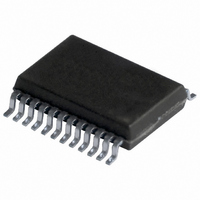
TDA9881TS/V5,118 NXP Semiconductors, TDA9881TS/V5,118 Datasheet - Page 11

TDA9881TS/V5,118
Manufacturer Part Number
TDA9881TS/V5,118
Description
IC IF-PLL DEMOD 24SSOP
Manufacturer
NXP Semiconductors
Type
Demodulatorr
Datasheet
1.TDA9881HNV5118.pdf
(42 pages)
Specifications of TDA9881TS/V5,118
Package / Case
24-SSOP
Applications
Set-Top Boxes
Mounting Type
Surface Mount
Maximum Operating Temperature
+ 70 C
Maximum Power Dissipation
385 mW
Minimum Operating Temperature
- 20 C
Modulation Type
Quadrature
Mounting Style
SMD/SMT
Operating Supply Voltage
5 V
Supply Current
70 A
Lead Free Status / RoHS Status
Lead free / RoHS Compliant
Lead Free Status / RoHS Status
Lead free / RoHS Compliant, Lead free / RoHS Compliant
Other names
935288679118
Philips Semiconductors
9397 750 13417
Product data sheet
8.13 Audio amplifier and mute time constant
8.14 Internal voltage stabilizer
8.15 Logic
The audio amplifier consists of two parts:
The AF preamplifier used for FM sound is an operational amplifier with internal feedback,
high gain and high common mode rejection. The AF voltage from the PLL demodulator is
5 mV (RMS) for a frequency deviation of 27 kHz and is amplified by 30 dB. By using a
DC operating point control circuit (with external capacitor C
decoupled from the PLL DC voltage. The low-pass characteristic of the amplifier reduces
the harmonics of the sound intercarrier signal at the AF output terminal.
For FM sound a switchable de-emphasis network (with external capacitor) is implemented
between the preamplifier and the output amplifier. The de-emphasis time constant with
50 s or 75 s depends on the FM carrier selection via pins FM0 and FM1; see
The AF output amplifier provides the required AF output level by a rail-to-rail output stage.
A preceding stage makes use of an input selector for switching between the FM sound
and mute state.
Switching to the mute state is controlled automatically, depending on the digital acquisition
help circuit should the VCO of the FM PLL not be in the required frequency window. This
is done by a time constant: fast for switching to the mute state and slow (typically 40 ms)
for switching to the non-mute state.
Auto mute can be disabled via pin AMUTE0; see
The band gap circuit internally generates a voltage of approximately 2.4 V, independent of
the supply voltage and the temperature. A voltage regulator circuit, connected to this
voltage, produces a constant voltage of 3.55 V which is used as an internal reference
voltage.
The logic circuit detects the logic level at the logic ports VIF0, QSSO, FM0, FM1 and
AMUTE0 and controls the internal functions; see
logic ports are open-circuit (high-ohmic or CMOS HIGH level) TV standard NTSC with a
vision carrier frequency of 45.75 MHz, an FM sound carrier frequency of 4.5 MHz,
de-emphasis with 75 s time constant and auto mute on is selected.
Table 4:
QSSO
No resistor at pin
No resistor at pin
2.2 k resistor to ground at pin pin open-circuit
2.2 k resistor to ground at pin pin connected to ground
•
•
AF preamplifier
AF output amplifier.
VIF frequency selection
Rev. 01 — 16 November 2004
Alignment-free vision and FM sound IF PLL demodulator
VIF0
pin open-circuit
pin connected to ground
Table
Table 4
6.
to
© Koninklijke Philips Electronics N.V. 2004. All rights reserved.
AF
Table
VIF frequency (MHz)
45.75
38.9
58.75
38.0
), the AF preamplifier is
6. In the event that all
TDA9881
Table
11 of 42
5.


