IP4771CZ16,118 NXP Semiconductors, IP4771CZ16,118 Datasheet
IP4771CZ16,118
Specifications of IP4771CZ16,118


Related parts for IP4771CZ16,118


IP4771CZ16,118 Summary of contents
Page 1
IP4770/71/72CZ16 VGA/video interface with integrated buffers, ESD protection and integrated termination resistors Rev. 01 — 25 October 2006 1. General description The IP4770CZ16, IP4771CZ16, IP4772CZ16 is connected between the VGA/DVI interface and the video graphics controller and includes level shifting ...
Page 2
... NXP Semiconductors 3. Applications I To terminate and to buffer channels, to reduce EMI/RFI and to provide downstream ESD protection for: N VGA interfaces including DDC channels N Desktop and notebooks PCs N Graphics cards N Set top boxes 4. Ordering information Table 1. Type number IP4770CZ16 IP4771CZ16 IP4772CZ16 5. Functional diagram V SYNC_IN1 SYNC_IN2 Fig 1 ...
Page 3
... NXP Semiconductors 6. Pinning information 6.1 Pinning Fig 2. Pin configuration 6.2 Pin description Table 2. Symbol V CC(SYNC) V CC(VIDEO) VIDEO_1 VIDEO_2 VIDEO_3 GND V CC(DDC) BYP DDC_OUT1 DDC_IN1 DDC_IN2 DDC_OUT2 SYNC_IN1 SYNC_OUT1 14 SYNC_IN2 SYNC_OUT2 16 IP4770CZ16_4771_4772_1 Product data sheet 1 V CC(SYNC CC(VIDEO) VIDEO_1 3 IP4770CZ16 4 VIDEO_2 ...
Page 4
... NXP Semiconductors 7. Limiting values Table 3. Limiting values In accordance with the Absolute Maximum Rating System (IEC 60134). Voltages are referenced to ground (GND). Symbol Parameter V electrostatic discharge voltage ESD V video supply voltage CC(VIDEO) V data display channel supply voltage CC(DDC) V synchronization supply voltage CC(SYNC) ...
Page 5
... NXP Semiconductors 8. Recommended operating conditions Table 4. Recommended operating conditions Symbol Parameter T operating temperature oper 9. Characteristics Table 5. Sync circuit characteristics unless otherwise specified. CC(SYNC) amb Symbol Parameter Supply: pin V CC(SYNC) I supply current on pin V CC(SYNC) Input: pins SYNC_IN1 and SYNC_IN2 V HIGH-level input voltage ...
Page 6
... NXP Semiconductors Table 6. Video circuit characteristics unless otherwise specified. CC(VIDEO) amb Symbol Parameter Supply: pin V CC(VIDEO) I supply current on pin V CC(VIDEO) Video channel: pins VIDEO_1, VIDEO_2 and VIDEO_3 C video channel capacitance ch(video) I video input current i(video) Protection diode V diode forward voltage ...
Page 7
... NXP Semiconductors 10. Application information The IP4770CZ16, IP4771CZ16, IP4772CZ16 should be placed as close as possible to the VGA/DVI interface connector. The ESD protection channels VIDEO_1, VIDEO_2 and VIDEO_3 can be connected in any order with RBG signals. The 100 k resistors between the DDC_OUTx channels and VCC_5V are optional. They may be used, if required, to pull-up the DDC_OUTx lines to VCC_5V when no monitor is connected to the VGA connector. Backfl ...
Page 8
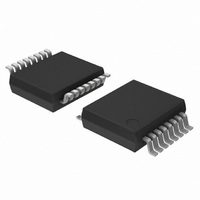
... NXP Semiconductors 11. Package outline SSOP16: plastic shrink small outline package; 16 leads; body width 3.9 mm; lead pitch 0.635 DIMENSIONS (mm are the original dimensions) A UNIT max. 0.25 1.55 mm 1.73 0.25 0.10 1.40 Note 1. Plastic or metal protrusions of 0.2 mm maximum per side are not included. ...
Page 9
... NXP Semiconductors 12. Abbreviations Table 8. Acronym CMOS DDC DVI EMI ESD FET HSYNC MOSFET PC RFI RGB SYNC TTL VGA VSYNC 13. Revision history Table 9. Revision history Document ID Release date IP4770CZ16_4771_4772_1 20061025 IP4770CZ16_4771_4772_1 Product data sheet Abbreviations Description Complementary Metal Oxide Semiconductor Data Display Channel ...
Page 10
... For detailed and full information see the relevant full data sheet, which is available on request via the local NXP Semiconductors sales office. In case of any inconsistency or conflict with the short data sheet, the full data sheet shall prevail ...
Page 11
... NXP Semiconductors 16. Contents 1 General description . . . . . . . . . . . . . . . . . . . . . . 1 2 Features . . . . . . . . . . . . . . . . . . . . . . . . . . . . . . . 1 3 Applications . . . . . . . . . . . . . . . . . . . . . . . . . . . . 2 4 Ordering information . . . . . . . . . . . . . . . . . . . . . 2 5 Functional diagram . . . . . . . . . . . . . . . . . . . . . . 2 6 Pinning information . . . . . . . . . . . . . . . . . . . . . . 3 6.1 Pinning . . . . . . . . . . . . . . . . . . . . . . . . . . . . . . . 3 6.2 Pin description . . . . . . . . . . . . . . . . . . . . . . . . . 3 7 Limiting values Recommended operating conditions Characteristics . . . . . . . . . . . . . . . . . . . . . . . . . . 5 10 Application information Package outline . . . . . . . . . . . . . . . . . . . . . . . . . 8 12 Abbreviations . . . . . . . . . . . . . . . . . . . . . . . . . . . 9 13 Revision history . . . . . . . . . . . . . . . . . . . . . . . . . 9 14 Legal information ...