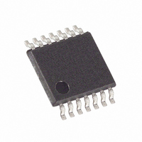
MAX11508UUD+ Maxim Integrated Products, MAX11508UUD+ Datasheet - Page 11

MAX11508UUD+
Manufacturer Part Number
MAX11508UUD+
Description
IC VID FILT HD/PS/SD/BP 14TSSOP
Manufacturer
Maxim Integrated Products
Type
Video Filterr
Datasheet
1.MAX11508UUD.pdf
(12 pages)
Specifications of MAX11508UUD+
Applications
DVD, Set-Top Boxes
Mounting Type
Surface Mount
Package / Case
14-TSSOP
Lead Free Status / RoHS Status
Lead free / RoHS Compliant
The MAX11508 filter characteristic provides excellent
time-domain response with low overshoot and guaran-
tees minimal attenuation in the passband. The
MAX11509 filters offer a small gain peaking response to
counter system rolloff.
Select filter frequency with inputs FSEL0 and FSEL1, as
shown in Table 1.
The MAX11508 SD filters have a 9MHz (typ) -3dB fre-
quency, while the MAX11509 SD filters offer a 10MHz
(typ) -3dB frequency and a +0.8dB high-frequency
boost at 5MHz (typ). Both devices have a stopband
attenuation of +48dB (typ) at 27MHz.
The MAX11508 PS filters have a 16MHz (typ) -3dB fre-
quency, while the MAX11509 PS filters offer a 17MHz
(typ) -3dB frequency and a +0.8dB high-frequency
boost at 8.5MHz (typ). Both devices have a stopband
attenuation of +44dB (typ) at 54MHz.
The MAX11508 HD filters have a 33MHz (typ) -3dB fre-
quency, while the MAX11509 HD filters offer a 34MHz
(typ) -3dB frequency and a +0.8dB high-frequency
boost at 20MHz (typ). Both devices have a stopband
attenuation of +45dB (typ) at 74.25MHz.
The MAX11508/MAX11509 filter bypass circuitry offers
a 60MHz (typ) -3dB frequency. Bypassed filters offer no
gain peaking.
The MAX11508/MAX11509 feature output buffers with
+6dB gain that drive a standard 150Ω video load at
2V
resistor, an optional 220µF or larger coupling capacitor,
and a 75Ω termination resistor.
An offset of 550mV is added at the output. The offset
ensures that the blanking level on the output is less
than 1V after the backmatch resistor, thus meeting digi-
tal TV specifications allowing the devices to drive video
loads directly without using costly AC-coupling capaci-
tors. The basic output voltage equation of all filters is:
Typical voltage waveforms are shown in Figures 2 and 3.
P-P
. A typical load consists of a 75Ω backmatch
Standard-Definition (SD) Filters
V
OUT
Progressive-Scan (PS) Filters
______________________________________________________________________________________
High-Definition (HD) Filters
= (2 x V
Bypassing the Filters
IN
) + 0.55V
Low-Cost, 3-Channel, HD/PS/SD/BP
Output Buffer
Filters
Video Filters with Buffer
Forcing digital input SHDN low places the MAX11508/
MAX11509 into low-power shutdown mode. In shut-
down, the device consumes only 1µA (typ), and the
outputs are internally connected to GND through
1.58kΩ resistors. In shutdown, the input clamps are dis-
abled and the inputs are internally connected to GND
through 350kΩ resistors. When shutdown is forced low
while BIAS is low, the bias network remains active, but
the bias voltage changes from its nominal 0.59V to
0.475V (typ).
DC- or AC-couple the MAX11508/MAX11509 outputs.
These devices, with +6dB gain, are typically connected
to a 75Ω series backmatch resistor followed by a video
cable. Choose an AC-coupling capacitor value that
ensures that the lowest frequency content in the video
signal is passed and the field-time distortion is kept
within desired limits when using an AC connection. The
selection of this value is a function of the input imped-
ance, and more importantly, the input leakage of the
circuit being driven. Common industry practice is to
use a 220µF or larger capacitor.
The MAX11508/MAX11509 outputs are fully protected
against short circuits to ground. The short-circuit pro-
tection circuitry limits the output current to 75mA (typ)
per output. Shorting more than one output to ground
simultaneously may exceed the maximum package
power dissipation.
Connect the power and ground traces to large copper
areas to enhance power dissipation. Bypass V
GND with 0.1µF and 1.0µF capacitors. Place the 0.1µF
capacitor closest to V
tors for their low inductance. Place traces carrying
video signals appropriately to avoid mutual coupling.
When inputs are AC-coupled, place the capacitors as
close as possible to the device and keep traces short
to minimize parasitic capacitance and inductance.
Refer to the MAX11508/MAX11509 evaluation kit data
sheet for PCB layout.
PROCESS: BiCMOS
Applications Information
PCB Layout Recommendations
CC
. Use surface-mount capaci-
Output Considerations
Chip Information
Shutdown
CC
11
to


