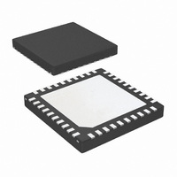
LMH1983SQE/NOPB National Semiconductor, LMH1983SQE/NOPB Datasheet - Page 8

LMH1983SQE/NOPB
Manufacturer Part Number
LMH1983SQE/NOPB
Description
IC VID CLK GEN MULTI RATE 40LLP
Manufacturer
National Semiconductor
Type
Clock Generatorr
Datasheet
1.LMH1983SQENOPB.pdf
(38 pages)
Specifications of LMH1983SQE/NOPB
Applications
Video Equipment
Mounting Type
Surface Mount
Package / Case
40-LLP
Leaded Process Compatible
Yes
Rohs Compliant
Yes
Interface Type
I2C
Supply Voltage (max)
3.3 V
Maximum Operating Temperature
+ 85 C
Minimum Operating Temperature
- 40 C
Mounting Style
SMD/SMT
Peak Reflow Compatible (260 C)
Yes
Lead Free Status / RoHS Status
Lead free / RoHS Compliant
Other names
LMH1983SQETR
Available stocks
Company
Part Number
Manufacturer
Quantity
Price
Part Number:
LMH1983SQE/NOPB
Manufacturer:
TI/德州仪器
Quantity:
20 000
www.national.com
VCXO Input (XOin)
Digital Holdover and Free-Run Specifications
V
V
Symbol
V
Note 1: Absolute Maximum Ratings are limits beyond which damage to the device may occur. Operating Ratings are conditions under which operation of the
device is intended to be functional. For guaranteed specifications and test conditions, see the Electrical Characteristics.
Note 2: Human Body Model, applicable std. MIL-STD-883, Method 3015.7. Machine Model, applicable std. JESD22-A115-A (ESD MM std. of JEDEC)
Field-Induced Charge-Device Model, applicable std. JESD22-C101-C (ESD FICDM std. of JEDEC).
Note 3: The maximum power dissipation is a function of T
T
Note 4: Electrical Table values apply only for factory testing conditions at the temperature indicated. No guarantee of parametric performance is indicated in the
electrical tables under conditions different than those tested.
Note 5: Typical values represent the most likely parametric norm as determined at the time of characterization. Actual typical values may vary over time and will
also depend on the application and configuration. The typical values are not tested and are not guaranteed on shipped production material.
Note 6: Limits are 100% production tested at 25°C. Limits over the operating temperature range are guaranteed through correlation using statistical analysis
methods.
Note 7: The SD and HD clock output jitter is based on XO input clock with 20 ps peak-to-peak using a time interval error (TIE) jitter measurement. The typical
TIE peak-to-peak jitter was measured on the LMH1983 evaluation bench board using TDSJIT3 jitter analysis software on a Tektronix DSA71604 oscilloscope
and 1 GHz active differential probe.
Note 8: t
the clock cycle where the input and output clocks are phase aligned.
Note 9: t
Note 10: The differential output swing and common mode voltage may be adjusted via the I
0x3Ah
Supported Standards and Timing Formats
Table 1
for the input and output formats. Auto-detection of the input is supported for the formats listed in
be manually programmed by the host via I
VCout_RNG
XOin_DIFF
A
XOin_SE
|V
|V
V
TDSJIT3 Clock TIE Measurement Setup: 10
Oscilloscope Setup: 20 mV/div vertical scale, 10 µs/div horizontal scale, and 25 GS/s sampling rate
V
f
)/ θ
I
I
T
OFF
t
OS
t
OZ
OD
OS
OD
OS
R
F
D
JA
|
|
. All numbers apply for packages soldered directly onto a PC Board.
D
D
lists the supported standard timing formats. The table includes the relevant parameters used to configure the LMH1983
for CLKoutX is measured from the positive clock edge of XOin to the positive clock edge of CLKoutX using 50% levels. The measurement is taken at
for FoutX is measured from the positive clock edge of CLKout to the negative edge of FoutX at the 50% levels
Duty Cycle
Rise Time
20% to 80%
Fall Time
80% to 20%
Differential Signal Output
Voltage
Common Signal Output Voltage 100Ω differential load, CLKout1, CLKout2
|Change to V
Complementary Output States
|Change to V
Complementary Output States
Output Short Circuit Current
Output Shutdown Leakage
Current
Maximum Relative Frequency
Offset between VCXO Input and
H Input
Single-ended Signal Input
Voltage Range
Differential Signal Input Voltage
Range
DAC Output Voltage Range
Parameter
OD
OS
| for
| for
-12
bit error rate (BER), >100K samples recorded using multiple acquisitions
2
C if its necessary to override the auto-detection feature.
Measured at 50% level of clock amplitude,
any output clock
15 pF load
15 pF load
100Ω differential load, CLKout1, CLKout2
or CLKout3
or CLKout3
100Ω differential load, CLKout1, CLKout2
or CLKout3
100Ω differential load, CLKout1, CLKout2
or CLKout3
Differential clock output pins connected to
GND for CLKout1, CLKout2 or CLKout3
Output buffer in shutdown mode, differential
clock output pins connected to V
Assumes H input jitter of ±15 ns
Single-ended input buffer mode
Differential input buffer mode, V
Digital Free-run Mode
J(MAX)
, θ
JA
. The maximum allowable power dissipation at any ambient temperature is PD = (T
(Note
(Note
(Note
(Note
Conditions
10)
10)
10)
10)
8
2
C interface. Testing is done with a value of 03Eh loaded into register
CM
DD
= 1.2V
or GND
(Note
1.125
Min
247
247
0.5
0
Table
6)
(Note
1. The input format can also
±150
1.25
Typ
400
400
350
350
50
1
5)
(Note
V
1.375
DD
Max
454
V
454
50
50
24
10
V
DD
-0.5
6)
J(MAX)
Units
|mV|
|mV|
|mA|
ppm
|µA|
mV
mV
ps
ps
%
V
V
V
–


