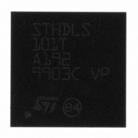
STHDLS101TQTR STMicroelectronics, STHDLS101TQTR Datasheet - Page 8

STHDLS101TQTR
Manufacturer Part Number
STHDLS101TQTR
Description
IC HDMI LEVEL SHIFTER AC 48-QFN
Manufacturer
STMicroelectronics
Type
Level Shifterr
Datasheet
1.STHDLS101TQTR.pdf
(26 pages)
Specifications of STHDLS101TQTR
Function
*
Circuit
*
On-state Resistance
*
Voltage Supply Source
*
Voltage - Supply, Single/dual (±)
*
Current - Supply
*
Operating Temperature
*
Mounting Type
Surface Mount
Package / Case
48-QFN
Applications
Graphic Cards, VGA Interfaces
Maximum Operating Temperature
+ 85 C
Minimum Operating Temperature
- 40 C
Mounting Style
SMD/SMT
Lead Free Status / RoHS Status
Lead free / RoHS Compliant
Other names
497-8499-2
Available stocks
Company
Part Number
Manufacturer
Quantity
Price
Company:
Part Number:
STHDLS101TQTR
Manufacturer:
AD
Quantity:
259
Pin configuration
3.1
8/26
Pin description
Table 2.
number
Pin
6
1
2
3
4
5
7
8
9
HPD_SOURCE
SDA_SOURCE
SCL_SOURCE
FUNCTION1
FUNCTION2
Pin description
VCC33
Name
REXT
GND
GND
Vendor-specific
Vendor-specific
control or test
control or test
Analog
Output
Power
Power
Power
Type
Input
pins
pins
I/O
Ground
3.3V±10% DC supply
Function pins are to enable vendor-specific features or
test modes.
For normal operation, these pins are tied to GND or
VCC33.
For consistent interoperability, GND is the preferred
default connection for these signals
Function pins are to enable vendor-specific features or
test modes.
For normal operation, these pins are tied to GND or
VCC33.
For consistent interoperability, GND is the preferred
default connection for these signals
Ground
Connection to external resistor. Resistor value
specified by device manufacturer.
Acceptable connections to this pin are:
- Resistor to GND
- Resistor to 3.3V;
- NC (direct connections to V
0-Ù resistor for layout compatibility
Buffer from the 0 V to 5 V input signal. The output
buffer stage is configurable based on the FUNCTION3
pin settings as desribed in the table below:
3.3 V DDC data I/O. Pulled-up by external termination
to 3.3 V. Connected to SDA_SINK through voltage-
limiting integrated NMOS pass-gate
3.3 V DDC clock I/O. Pulled-up by external termination
to 3.3 V. Connected to SCL_SINK through voltage-
limiting integrated NMOS pass-gate
FUNCTION3
0
0
1
1
HPD_SINK
Function
High (5 V)
High (5 V)
Low (0 V)
Low
CC
or GND are through a
external pull up to
HPD_SOURCE
(normally 1 V)
connected an
Open-drain,
STHDLS101T
the desired
High (3 V)
Low (0 V)
Low (0 V)
supply


