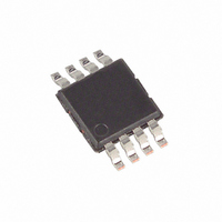
MAX9691EUA+ Maxim Integrated Products, MAX9691EUA+ Datasheet - Page 6

MAX9691EUA+
Manufacturer Part Number
MAX9691EUA+
Description
IC COMPARATOR W/LE 8-UMAX
Manufacturer
Maxim Integrated Products
Type
General Purposer
Datasheet
1.MAX9691ESA.pdf
(10 pages)
Specifications of MAX9691EUA+
Number Of Elements
1
Output Type
Complementary, ECL
Mounting Type
Surface Mount
Package / Case
8-TSSOP, 8-MSOP (0.118", 3.00mm Width)
Number Of Channels
1 Channel
Product
Analog Comparators
Offset Voltage (max)
+/- 11.5 mV
Input Bias Current (max)
30 uA
Supply Voltage (max)
10.5 V
Supply Voltage (min)
9.5 V
Supply Current (max)
26000 uA
Maximum Power Dissipation
330 mW
Maximum Operating Temperature
+ 85 C
Mounting Style
SMD/SMT
Minimum Operating Temperature
- 40 C
Comparator Type
General Purpose
No. Of Comparators
1
Response Time
1.2ns
Ic Output Type
ECL, Open Emitter
Supply Current
18mA
Supply Voltage Range
4.5V To 5.5V
Amplifier Case Style
µMAX
Rohs Compliant
Yes
Lead Free Status / RoHS Status
Lead free / RoHS Compliant
As high-speed receivers, the MAX9691/MAX9692/
MAX9693 are capable of processing signals in excess
of 600MHz. Figure 2 is a 100MHz example with an
input signal level of 14mV
The timing diagram (Figure 3) illustrates the series of
events that complete the compare function, under
worst-case conditions. The top line of the diagram illus-
Single/Dual, Ultra-Fast, ECL-Output
Comparators with Latch Enable
Figure 2. Signal Processed at 100MHz with Input Signal Level
of 14mV
Figure 3. Timing Diagram
6
500mV/div
20mV/div
OUTPUT
_______________________________________________________________________________________
INPUT
RMS
DIFFERENTIAL
VOLTAGE
ENABLE
LATCH
INPUT
Q
Q
LATCH
V
RMS
IN
2ns/div
.
COMPARE
V
OD
t
s
t h
t
pd
-1.7V
0V
-0.9V
trates two latch-enable pulses. Each pulse is high for
the compare function and low for the latch function. The
first pulse demonstrates the compare function; part of
the input action takes place during the compare mode.
The second pulse demonstrates a compare function
interval during which there is no change in the input.
The leading edge of the input signal (illustrated as a
large-amplitude, small-overdrive pulse) switches the
comparator after time interval t
sistors are similar in timing. The input signal must occur
at time t
maintained for time t
After t
tus until the latch is again strobed. A minimum latch
pulse width of t
tion, and the output transitions occur after a time t
The MAX9691/MAX9692/MAX9693 will not false trip
(i.e., output invert) if one of the inputs is in the valid
common-mode range while the other input is outside
the common-mode range.
h
, the output is no longer affected by the input sta-
s
before the latch falling edge, and must be
t
pw(LE)
t
LE(+)
pw(LE)
h
is needed for the strobe opera-
after the edge to be acquired.
pd
. Output Q and Q tran-
50%
V
50%
50%
OS
LE(±)
.


