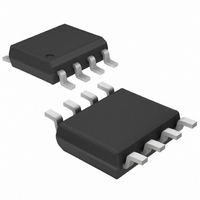
MAX9109ESA+T Maxim Integrated Products, MAX9109ESA+T Datasheet - Page 7

MAX9109ESA+T
Manufacturer Part Number
MAX9109ESA+T
Description
IC COMPAR LP SNGL 8-SOIC
Manufacturer
Maxim Integrated Products
Type
with Latchr
Datasheet
1.MAX9109EUTT.pdf
(13 pages)
Specifications of MAX9109ESA+T
Number Of Elements
1
Output Type
TTL
Voltage - Supply
4.5 V ~ 5.5 V
Mounting Type
Surface Mount
Package / Case
8-SOIC (0.154", 3.90mm Width)
Lead Free Status / RoHS Status
Lead free / RoHS Compliant
Because of the MAX9107/MAX9108/MAX9109’s high
gain bandwidth, special precautions must be taken to
realize the full high-speed capability. A printed circuit
board with a good, low-inductance ground plane is
mandatory. Place the decoupling capacitor (a 0.1µF
ceramic capacitor is a good choice) as close to V
possible. Pay close attention to the decoupling capaci-
tor’s bandwidth, keeping leads short. Short lead
lengths on the inputs and outputs are also essential to
avoid unwanted parasitic feedback around the com-
parators. Solder the device directly to the printed circuit
board instead of using a socket.
The inputs to the MAX9107/MAX9108/MAX9109 may be
driven beyond the voltage limits given in the Absolute
Maximum Ratings, as long as the current flowing into the
device is limited to 25mA. However, if the inputs are over-
driven, the output may be inverted. The addition of an
external diode prevents this inversion by limiting the input
voltage to 200mV to 300mV below ground (see Figure 3).
In Figure 4, the circuit allows reception of infrared data.
The MAX4400 converts the photodiode current to a
voltage, and the MAX9109 determines whether the
amplifier output is high enough to be called a “1.” The
current consumption of this circuit is minimal: the
MAX4400 and MAX9109 require typically 410µA and
350µA, respectively.
Figure 1. Input and Output Waveforms, Noninverting Input
Varied
V
V
COMPARATOR
V
TRIP+
TRIP-
HYST
Battery-Operated Infrared Data Link
OUTPUT
Applications Information
_______________________________________________________________________________________
Overdriving the Inputs
25ns, Dual/Quad/Single, Low-Power,
V
IN+
Circuit Layout
V
V
OS
IN-
=
= 0
V
TRIP+
V
V
OH
OL
2
+ V
TRIP-
CC
as
Figure 2. MAX9109 Timing Diagram
Figure 3. Schottky Clamp for Input Driven Below Ground
Figure 4. Battery-Operated Infrared Data Link Consumes Only
760µA
DIFFERENTIAL
VOLTAGE
OUTPUT
INPUT
I
SRC
V
LE
CLAMP
SIEMENS BP-104
PHOTODIODE
1000pF
100kΩ
1.4V
= -200mV TO -300mV
1.4V
V
V
V
V-
3V
OH
OS
OL
MAX4400
0
TTL Comparators
COMPARE
1000pF
47kΩ
3
1
10pF
1MΩ
+5V
t
s
V
V
IN
OD
100kΩ
t
2
h
5
t
PD
LATCH
+
4
+5V
0.1µF
3
4
+5V
2
1/2 MAX9107
6
MAX9109
5
1
DATA
0.1µF
7


