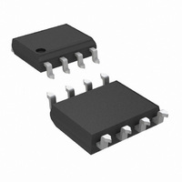
LMC7215IMX/NOPB National Semiconductor, LMC7215IMX/NOPB Datasheet - Page 6

LMC7215IMX/NOPB
Manufacturer Part Number
LMC7215IMX/NOPB
Description
IC COMP MICRPWR R-R CMOS 8-SOIC
Manufacturer
National Semiconductor
Type
General Purposer
Datasheet
1.LMC7225IM5NOPB.pdf
(11 pages)
Specifications of LMC7215IMX/NOPB
Number Of Elements
1
Output Type
Push-Pull
Voltage - Supply
2 V ~ 8 V, ±1 V ~ 4 V
Mounting Type
Surface Mount
Package / Case
8-SOIC (0.154", 3.90mm Width)
Lead Free Status / RoHS Status
Lead free / RoHS Compliant
Other names
*LMC7215IMX
*LMC7215IMX/NOPB
LMC7215IMX
LMC7215IMXTR
*LMC7215IMX/NOPB
LMC7215IMX
LMC7215IMXTR
www.national.com
Application Information
RESPONSE TIME
Depending upon the amount of overdrive, the delay will
typically be between 10 µs to 200 µs. The curve showing
delay vs. overdrive in the “Typical Characteristics” section
shows the delay time when the input is preset with 100 mV
across the inputs and then is driven the other way by 1 mV
to 500 mV.
The transition from high to low or low to high is fast. Typically
1 µs rise and 400 ns fall.
With a small signal input, the comparators will provide a
square wave output from sine wave inputs at frequencies as
high as 25 kHz. Figure 1 shows a worst case example where
a
output is delayed by almost 180˚.
NOISE
Most comparators have rather low gain. This allows the
output to spend time between high and low when the input
signal changes slowly. The result is the output may oscillate
between high and low when the differential input is near
zero.
The exceptionally high gain of these comparators, 10,000
V/mV, eliminates this problem. Less then 1 µV of change on
the input will drive the output from one rail to the other rail.
If the input signal is noisy, the output cannot ignore the noise
unless some hysteresis is provided by positive feedback.
±
5 mV sine wave is applied to the input. Note that the
FIGURE 1.
FIGURE 2.
01285305
01285304
6
INPUT VOLTAGE RANGE
The LMC7215/25 have input voltage ranges that are larger
than the supply voltage guarantees that signals from other
parts of the system cannot overdrive the inputs. This allows
sensing supply current by connecting one input directly to
the V
resistor. The same is true if the sense resistor is in the
ground return line.
Sensing supply voltage is also easy by connecting one input
directly to the supply.
The inputs of these comparators are protected by diodes to
both supplies. This protects the inputs from both ESD as well
as signals that greatly exceed the supply voltages. As a
result, current will flow through these forward biased diodes
whenever the input voltage is more than a few hundred
millivolts larger than the supplies. Until this occurs, there is
essentially no input current. As a result, placing a large
resistor in series with any input that may be exposed to large
voltages, will limit the input current but have no other notice-
able effect.
If the input current is limited to less than 5 mA by a series
resistor, (see Figure 2), a threshold or zero crossing detec-
tor, that works with inputs from as low as a few millivolts to as
high as 5,000V, is made with only one resistor and the
comparator.
INPUTS
As mentioned above, these comparators have near zero
input current. This allows very high resistance circuits to be
used without any concern for matching input resistances.
This also allows the use of very small capacitors in R-C type
timing circuits. This reduces the cost of the capacitors and
amount of board space used.
CAPACITIVE LOADS
The high output current drive allows large capacitive loads
with little effect. Capacitive loads as large as 10,000 pF have
no effect upon delay and only slow the transition by about 3
µs.
OUTPUT CURRENT
Even though these comparators use less than 1 µA supply
current, the outputs are able to drive very large currents.
The LMC7215 can source up to 50 mA when operated on a
5V supply. Both the LMC7215 and LMC7225 can sink over
20 mA. (See the graph of Max I
Characteristics” section.)
This large current handling ability allows driving heavy loads
directly. LEDs, beepers and other loads can be driven easily.
The push-pull output stage of the LMC7215 is a very impor-
tant feature. This keeps the total system power consumption
to the absolute minimum. The only current consumed is the
less than 1 µA supply current and the current going directly
into the load. No power is wasted in a pull-up resistor when
the output is low. The LMC7225 is only recommended where
a level shifting function from one logic level to another is
desired, where the LMC7225 is being used as a drop-in
lower power replacement for an older comparator or in cir-
cuits where more than one output will be paralleled.
+
line and the other to the other side of a current sense
O
vs. V
SUPPLY
in the “Typical


