MC3302PG ON Semiconductor, MC3302PG Datasheet - Page 4
MC3302PG
Manufacturer Part Number
MC3302PG
Description
IC COMP QUAD SINGLE SUPPLY 14DIP
Manufacturer
ON Semiconductor
Type
General Purposer
Specifications of MC3302PG
Number Of Elements
4
Output Type
CMOS, Open-Collector, TTL
Voltage - Supply
3 V ~ 30 V, ±1.5 V ~ 15 V
Mounting Type
Through Hole
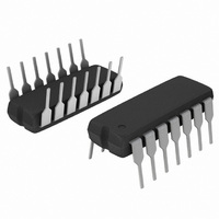
Package / Case
14-DIP (0.300", 7.62mm)
Number Of Channels
4 Channels
Response Time
1.3 us
Offset Voltage (max)
20 mV
Input Bias Current (max)
500 nA
Supply Voltage (max)
30 V
Supply Voltage (min)
3 V
Supply Current (max)
2.5 mA
Maximum Power Dissipation
1000 mW
Maximum Operating Temperature
+ 85 C
Mounting Style
Through Hole
Minimum Operating Temperature
- 40 C
Amplifier Type
Comparator
Current, Input Bias
25 nA
Current, Input Offset
±3 nA
Current, Supply
1 mA
Number Of Amplifiers
Quad
Package Type
SOIC-14
Power Dissipation
1 W
Temperature, Operating, Range
-40 to +85 °C
Voltage, Gain
100 V/mV
Voltage, Input Offset
±3 mVDC
Voltage, Supply
±18 VDC
Comparator Type
General Purpose
No. Of Comparators
4
Ic Output Type
CMOS, TTL
Supply Current
1mA
Supply Voltage Range
3V To 30V
Amplifier Case Style
DIP
No. Of Pins
14
Rohs Compliant
Yes
Output Compatibility
CMOS, TTL
Lead Free Status / RoHS Status
Lead free / RoHS Compliant
Other names
MC3302PGOS
Available stocks
Company
Part Number
Manufacturer
Quantity
Price
Company:

Part Number:
MC3302PG
Manufacturer:
ON
Quantity:
7 700
Company:
Part Number:
MC3302PG
Manufacturer:
ON Semiconductor
Quantity:
4


7. (LM239) T
8. At the output switch point, V
9. The bias current flows out of the inputs due to the PNP input stage. This current is virtually constant, independent of the output state.
10. The response time specified is for a 100 mV input step with 5.0 mV overdrive. For larger signals, 300 ns is typical.
PERFORMANCE CHARACTERISTICS
+ V
Input Offset Voltage (Note 8)
Input Bias Current (Notes 8, 9)
Input Offset Current (Note 8)
Input Common Mode Voltage Range
Saturation Voltage
Output Leakage Current
Differential Input Voltage
(LM339) T
(MC3302) T
(LM2901) T
(LM2901V & NCV2901) T
NCV2901 is qualified for automotive use.
(0 Vdc to V
(Output in Analog Range)
V
I
V
V
All V
sink
V
CC
I
I
O
in
(−) ≥ +1.0 Vdc, V
(+) ≥ +1.0 Vdc, V
= 30 Vdc
≤ 4.0 mA
I
≥ 0 Vdc
10 k
low
low
R
Figure 2. Inverting Comparator
R3
CC
ref
low
low
V
10k
Characteristic
ref
= −25°C, T
= 0°C, T
−1.5 Vdc).
= −40°C, T
= −40°C, T
R1
with Hysteresis
I
I
+ V
+
(+) = 0,
-
(−) = 0,
high
1.0 M
R2
CC
high
low
high
= +70°C
high
O
V
R3 ] R1 / / R
V
R2
= +85°
= −40°C, T
ref
= +105°
] 1.4 Vdc, R
H
= +85°C
=
[
R1/ / R
Rref / / R1
10 k
R
V
R1 / / R
ref
CC
V
+ R1
O
R1
high
ref
ref
+ R2
ref
/ / R2
S
= +125°C
(V
≤ 100 W 5.0 Vdc ≤ V
CC
Symbol
[V
V
V
= +5.0 Vdc, T
V
O(max)
ICMR
I
V
I
I
OL
IB
IO
sat
IO
ID
- V
http://onsemi.com
O(min)
Min
−
−
−
0
−
−
−
]
A
LM239/339
= T
CC
4
Typ
low
−
−
−
−
−
−
−
≤ 30 Vdc, with the inputs over the full common mode range
Vi
R
ref
n
to T
±150
Max
±9.0
V
−2.0
V
400
700
1.0
R1
high
CC
CC
Figure 3. Noninverting Comparator
10 k
R2
V
ref
[Note 7])
Min
−
−
−
0
−
−
−
LM2901/2901V/
NCV2901
with Hysteresis
+
-
+ V
Typ
−
−
−
−
−
−
−
1.0 M
R3
CC
±200
Max
−2.0
V
V
±15
500
700
1.0
CC
CC
V
R2 [ R1 / / R
Amount of Hysteresis V
H
10 k
=
Min
R2 + R3
−
−
−
0
−
−
−
V
V
R2
ref
O
MC3302
=
Typ
ref
[(V
−
−
−
−
−
−
−
R
V
ref
CC
O(max)
+ R1
R1
1000
±300
Max
−2.0
V
V
H
±40
700
1.0
- V
CC
CC
O(min)
mVdc
Unit
Vdc
mV
]
nA
nA
mA
V
Related parts for MC3302PG
Image
Part Number
Description
Manufacturer
Datasheet
Request
R

Part Number:
Description:
ON Semiconductor [VOLTAGE REGULATOR]
Manufacturer:
ON Semiconductor
Datasheet:
Part Number:
Description:
357-036-542-201 CARDEDGE 36POS DL .156 BLK LOPRO
Manufacturer:
ON Semiconductor
Datasheet:
Part Number:
Description:
357-036-542-201 CARDEDGE 36POS DL .156 BLK LOPRO
Manufacturer:
ON Semiconductor
Datasheet:
Part Number:
Description:
357-036-542-201 CARDEDGE 36POS DL .156 BLK LOPRO
Manufacturer:
ON Semiconductor
Datasheet:
Part Number:
Description:
357-036-542-201 CARDEDGE 36POS DL .156 BLK LOPRO
Manufacturer:
ON Semiconductor
Datasheet:
Part Number:
Description:
357-036-542-201 CARDEDGE 36POS DL .156 BLK LOPRO
Manufacturer:
ON Semiconductor
Datasheet:
Part Number:
Description:
357-036-542-201 CARDEDGE 36POS DL .156 BLK LOPRO
Manufacturer:
ON Semiconductor
Datasheet:
Part Number:
Description:
357-036-542-201 CARDEDGE 36POS DL .156 BLK LOPRO
Manufacturer:
ON Semiconductor
Datasheet:
Part Number:
Description:
357-036-542-201 CARDEDGE 36POS DL .156 BLK LOPRO
Manufacturer:
ON Semiconductor
Datasheet:
Part Number:
Description:
357-036-542-201 CARDEDGE 36POS DL .156 BLK LOPRO
Manufacturer:
ON Semiconductor
Datasheet:
Part Number:
Description:
357-036-542-201 CARDEDGE 36POS DL .156 BLK LOPRO
Manufacturer:
ON Semiconductor
Datasheet:
Part Number:
Description:
Manufacturer:
ON Semiconductor
Datasheet:
Part Number:
Description:
Manufacturer:
ON Semiconductor
Datasheet:
Part Number:
Description:
Manufacturer:
ON Semiconductor
Datasheet: