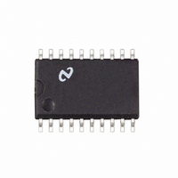
LM2202M National Semiconductor, LM2202M Datasheet - Page 6

LM2202M
Manufacturer Part Number
LM2202M
Description
IC VIDEO AMP SYSTEM 20-SOIC
Manufacturer
National Semiconductor
Datasheet
1.LM2202M.pdf
(17 pages)
Specifications of LM2202M
Applications
General Purpose
Number Of Circuits
1
-3db Bandwidth
230MHz
Current - Supply
48mA
Current - Output / Channel
28mA
Voltage - Supply, Single/dual (±)
8 V ~ 13.2 V
Mounting Type
Surface Mount
Package / Case
20-SOIC (0.300", 7.50mm Width)
Lead Free Status / RoHS Status
Contains lead / RoHS non-compliant
Other names
*LM2202M
Available stocks
Company
Part Number
Manufacturer
Quantity
Price
Part Number:
LM2202M
Manufacturer:
NS/国半
Quantity:
20 000
www.national.com
Circuit Description
VIDEO AMPLIFIER SECTION (Output Stage)
A simplified schematic of LM2202’s video amplifier output
stage is shown in Figure 4 . The output stage is the second
gain stage. Ideally the gain of the second gain stage would
be A
low open loop gain, the gain is approximately A
Thus the maximum gain of the video amplifier is A
A
to the load. The output voltage can swing from 0.2V to 10V.
CONTRAST CONTROL SECTION
A simplified schematic of LM2202’s contrast control section
is shown in Figure 5 . A 0V to 4V DC voltage is applied at the
contrast input (pin 8). Transistors Q29, Q30 and Q34 buffer
and level shift the contrast voltage to the base of Q36. The
voltage at the emitter of Q36 equals the contrast voltage
(V
I
Transistor Q36’s collector current is used to unbalance the
current through the differential pair comprised of Q38 and
Q40. Q40’s base is internally biased at 5.3V and made avail-
C36
V2
cont
= 20. Transistors Q23 and Q24 provide a push-pull drive
V2
= V
) and the current through Q36’s collector is given by
= −R21/R18 = −16. Because of the output stage’s
cont
/R28.
FIGURE 3. Simplified Schematic of the LM2202 Video Amplifier Input Stage
(Continued)
V
V2
= A
= −10.
V1
x
6
able at pin 20. Pin 20 is externally connected to pin 1 through
a 100
Q38 (pin 3) is externally connected to pin 2 through a 100
resistor (see Figure 2 and Figure 3 ). With V
ferential pair (Q38, Q40) is balanced and the voltage at pins
1 and 2 is 5.3V. Under this condition, Q8’s collector current is
equally split between Q9 and Q10 (see Figure 3 ) and the
amplifier’s gain is half the maximum gain. If contrast voltage
at pin 8 is greater than 2V then Q36’s collector current in-
creases, thus pulling Q38’s collector node lower and conse-
quently moving Q38’s base below 5.3V. With pin 2 at a lower
voltage than pin 1, current through Q10 (see Figure 3 ) in-
creases and the amplifier’s gain increases. With V
the amplifier’s gain is maximum.
If the contrast voltage at pin 8 is less than 2V then Q36’s col-
lector current decreases and Q38’s base is pulled above
5.3V. With pin 2 voltage greater than pin 1 voltage, less cur-
rent flows through Q10 (see Figure 3 ), consequently the am-
plifier’s gain decreases. With V
is minimum (i.e., maximum attenuation).
resistor (see Figure 2 and Figure 3 ). The base of
cont
= 0V, the amplifier’s gain
cont
= 2V, the dif-
cont
DS012591-9
= 4V,


