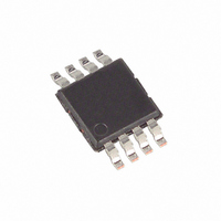
MAX9651AUA+T Maxim Integrated Products, MAX9651AUA+T Datasheet - Page 6

MAX9651AUA+T
Manufacturer Part Number
MAX9651AUA+T
Description
IC OPAMP VCOM DRIVE 8-UMAX-EP
Manufacturer
Maxim Integrated Products
Datasheet
1.MAX9650AUA.pdf
(13 pages)
Specifications of MAX9651AUA+T
Applications
TFT-LCD Panels: VCOM Driver
Output Type
Rail-to-Rail
Number Of Circuits
2
-3db Bandwidth
35MHz
Slew Rate
40 V/µs
Current - Supply
3.7mA
Current - Output / Channel
1.3A
Voltage - Supply, Single/dual (±)
9 V ~ 20 V, ±4.5 V ~ 10 V
Mounting Type
Surface Mount
Package / Case
8-TSSOP, 8-MSOP (0.118", 3.00mm Width), Exposed Pad
Lead Free Status / RoHS Status
Lead free / RoHS Compliant
High-Current VCOM Drive Op Amps
for TFT LCDs
The MAX9650/MAX9651 are designed to drive capaci-
tive loads. A small value of series resistance improves
the performance of the device to ensure stability and
fast settling with very large or very small capacitive
loads. In many cases, this resistance is already present
due to connection resistance in the wiring and no addi-
tional physical resistor is necessary. For minimum
series resistance required for stability with capacitive
loading, see Figure 2.
The MAX9650/MAX9651 operate from a 6V to 20V sin-
gle supply or from ±4.5V to ±10V dual supplies. Proper
supply bypassing ensures stability while driving high
Figure 2. Minimum Combined ESR/Series/Trace Resistance
Required for Stability of the MAX9650 in Response to
Capacitive Loads
µMAX is a registered trademark of Maxim Integrated Products, Inc.
6
_______________________________________________________________________________________
Power Supplies and Bypass Capacitors
2.0
1.8
1.6
1.4
1.2
1.0
0.8
0.6
0.4
0.2
0
10
-7
Applications Information
UNSTABLE
10
CAPACITANCE (F)
-6
STABLE
10
-5
Output Load
10
-4
transient loads. The MAX9650/MAX9651 require a mini-
mum 10µF (C1) and 0.1µF (C2) power-supply bypass
capacitors placed as close as possible to the power-
supply pin (V
tion, use 10µF and 0.1µF bypass capacitors on both
supplies (V
close as possible to V
The exposed pad on the µMAX
provide a low thermal resistance for heat dissipation.
Solder the exposed pad to a ground plane for best
thermal performance. Do not route traces under these
packages. For dual-supply operation, the exposed pad
(EP) can be electrically connected to the negative sup-
ply or it can be left unconnected.
Figure 3. Typical TFT-LCD Backplane Drive Circuit
PROCESS: BiCMOS
V
REF
SUPPLY
19V
**R
*10μF and 0.1μF CAPACITORS AS CLOSE AS POSSIBLE TO THE PIN.
*C2 = 0.1μF
S
MAY BE NEEDED FOR SOME APPLICATIONS.
DD
IN_+
IN_-
DD
SUPPLY
and GND) with each capacitor placed as
16V
). See Figure 3. For dual-supply opera-
MAX9650
GND
V
DD
DD
and GND.
OUT_
*C1 = 10μF
Layout and Grounding
Chip Information
®
**R
S
and TDFN packages
TFT LCD
TFT-LCD
CAPACITANCE


