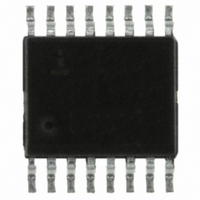
ISL59837IAZ Intersil, ISL59837IAZ Datasheet - Page 13

ISL59837IAZ
Manufacturer Part Number
ISL59837IAZ
Description
IC VIDEO DRIVER TRUE SGL 16-QSOP
Manufacturer
Intersil
Datasheet
1.ISL59837IAZ.pdf
(14 pages)
Specifications of ISL59837IAZ
Applications
Voltage Feedback
Output Type
Rail-to-Rail
Number Of Circuits
3
-3db Bandwidth
200MHz
Slew Rate
500 V/µs
Current - Supply
97mA
Current - Output / Channel
80mA
Voltage - Supply, Single/dual (±)
3 V ~ 3.6 V
Mounting Type
Surface Mount
Package / Case
16-QSOP
Lead Free Status / RoHS Status
Lead free / RoHS Compliant
Available stocks
Company
Part Number
Manufacturer
Quantity
Price
Part Number:
ISL59837IAZ
Manufacturer:
INTERSIL
Quantity:
20 000
Company:
Part Number:
ISL59837IAZ-T7
Manufacturer:
Intersil
Quantity:
800
designed to drive three channels; simply deal with each
channel separately as described in this section.
DC-RESTORE
When the ISL59837 is AC-coupled it becomes necessary to
restore the DC reference for the signal. This is accomplished
with a DC-restore system applied between the capacitive
"AC" coupling and the input of the device. Refer to
“ISL59837 + DC-Restore Solution” on page 10.
DISABLE/POWER-DOWN
The ISL59837 can be disabled and its output placed in a
high impedance state. The turn-off time is around 25ns and
the turn-on time is around 200ns. When the PD pin is taken
high, the chip’s total supply current is reduced to 0.1mA
typically, all but eliminating the power used by the part.
Taking the EN pin high powers down the amplifiers, leaving
the charge pump running. Both pins can be controlled by
standard TTL or CMOS signal levels (0.8V V
relative to GND).
OUTPUT DRIVE CAPABILITY
The ISL59837 does not have internal short-circuit protection
circuitry. A short-circuit current of 80mA sourcing and 150mA
sinking for the output is connected half way between the rails
with a 10Ω resistor. If the output is shorted indefinitely, the
power dissipation could easily increase such that the part will
be destroyed. Maximum reliability is maintained if the output
current never exceeds ±40mA, after which the electro-migration
limit of the process will be exceeded and the part will be
damaged. This limit is set by the design of the internal metal
interconnections.
POWER DISSIPATION
With the high output drive capability of the ISL59837, it is
possible to exceed the
temperature under certain load current conditions.
Therefore, it is important to calculate the maximum junction
temperature for an application to determine if load conditions
or package types need to be modified to assure operation of
the amplifier in a safe operating area.
The maximum power dissipation allowed in a package is
determined according to Equation 1:
Where:
The maximum power dissipation actually produced by an IC
is the total quiescent supply current times the total power
supply voltage, plus the power in the IC due to the load, or:
PD
T
T
θ
MAX
AMAX
JA
JMAX
= Thermal resistance of the package
=
= Maximum junction temperature
= Maximum ambient temperature
T
-------------------------------------------- -
JMAX
θ
–
JA
T
AMAX
+
150°C absolute maximum junction
13
IL
, 2.0V V
(EQ. 1)
IH
ISL59837
for sourcing:
for sinking:
Where:
By setting the two P
can solve the output current and R
overheat.
Power Supply Bypassing and Printed Circuit
Board Layout
Strip line design techniques are recommended for the input
and output signal traces. As with any high frequency device,
a good printed circuit board layout is necessary for optimum
performance. Lead lengths should be as short as possible.
The power supply pin must be well bypassed to reduce the
risk of oscillation. For normal single supply operation, where
the V
tantalum capacitor in parallel with a 0.1µF ceramic capacitor
from V
combination should be placed at each supply pin to ground if
split-internal supplies are to be used. In this case, the V
pin becomes the negative supply rail.
For good AC performance, parasitic capacitance should be
kept to a minimum. Use of wire-wound resistors should be
avoided because of their additional series inductance. Use
of sockets should also be avoided if possible. Sockets add
parasitic inductance and capacitance can result in
compromised performance. Minimizing parasitic capacitance
at the amplifier's inverting input pin is also very important.
PD
PD
V
I
V
R
I
i = Number of output channels
SMAX
LOAD
MAX
MAX
S
OUT
LOAD
S
= Supply voltage
- pin is connected to the ground plane, a single 4.7µF
S
+ to GND will suffice. This same capacitor
=
=
= Maximum output voltage of the application
= Load current
= Maximum quiescent supply current
= Load resistance tied to ground
V
V
S
S
×
×
I
I
SMAX
SMAX
DMAX
+
+
(
(
V
V
S
OUT
equations equal to each other, we
–
V
i V
OUT
–
S
i
LOAD
)
)
×
×
V
-----------------
I
LOAD
OUT
R
to avoid the device
L
i
i
i
March 5, 2007
FN6335.1
(EQ. 2)
(EQ. 3)
S
-


