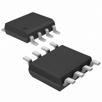
MAX9005ESA+T Maxim Integrated Products, MAX9005ESA+T Datasheet - Page 2

MAX9005ESA+T
Manufacturer Part Number
MAX9005ESA+T
Description
IC OP AMP LP HI SPEED 8-SOIC
Manufacturer
Maxim Integrated Products
Type
Amplifier, Comparatorr
Datasheet
1.MAX9002EUA.pdf
(20 pages)
Specifications of MAX9005ESA+T
Applications
General Purpose
Mounting Type
Surface Mount
Package / Case
8-SOIC (3.9mm Width)
Lead Free Status / RoHS Status
Lead free / RoHS Compliant
ABSOLUTE MAXIMUM RATINGS
Supply Voltage (V
Voltage Inputs (AIN_, CIN_).............(V
Output Short-Circuit Duration (AOUT, COUT, REF) ...Continuous
Continuous Power Dissipation (T
Low-Power, High-Speed, Single-Supply
Op Amp + Comparator + Reference ICs
Stresses beyond those listed under “Absolute Maximum Ratings” may cause permanent damage to the device. These are stress ratings only, and functional
operation of the device at these or any other conditions beyond those indicated in the operational sections of the specifications is not implied. Exposure to
absolute maximum rating conditions for extended periods may affect device reliability.
ELECTRICAL CHARACTERISTICS
(V
MAX9001/MAX9002/MAX9004/MAX9005), COUT = low, I
at V
2
Supply Voltage Range
Supply Current
Supply Current in
Shutdown
Shutdown Input Bias
Current
Shutdown Logic High
Shutdown Logic Low
OP AMP
Input Offset Voltage
Input Offset Voltage
Temperature Coefficient
Input Bias Current
Input Offset Current
Input Resistance
Input Common-Mode
Voltage Range
Common-Mode
Rejection Ratio
Power-Supply Rejection
Ratio
Output Resistance
Output Short-Circuit
Current
Disabled Mode Output
Leakage
8-Pin SO (derate 5.88mW/°C above +70°C).................471mW
8-Pin µMAX (derate 4.1mW/°C above +70°C) ..............330mW
DD
DD
_______________________________________________________________________________________
= +2.5V to +5.5V, V
PARAMETER
= 5V and T
DD
A
= +25°C.)
to V
SS
SS
) ....................................-0.3V to +6V
= 0,
V
(DISABLED)
SYMBOL
V
I
IN( SHDN )
IH( SHDN )
IL( SHDN )
TCV
CMVR
CMRR
A
I
PSRR
I
SHDN
I
V
V
I
BIAS
R
OUT
DD
= +70°C)
SHDN = V
DD
OS
IN
OS
SS
- 0.3V) to (V
to either V
Guaranteed by PSRR tests
MAX9000/MAX9001/
MAX9003/MAX9004
MAX9002/MAX9005
MAX9001/MAX9004 (V
MAX9001/MAX9004 (V
MAX900_ES_
MAX900_ES_
AIN+, AIN-
AIN+, AIN-
Differential or common mode
Guaranteed by CMRR test
MAX900_ES_, (V
V
V
A
Shorted to V
Shorted to V
V
DD
DD
DD
V
SHDN
= 1V/V
(MAX9001/MAX9004 only), V
= 5.5V
= 2.5V to 5.5V
≤ (0.3V x V
DD
SS
+ 0.3V)
SS
DD
or V
OUT(REF)
DD
SS
CONDITIONS
DD
- 0.15V) ≤ V
), V
= 0, T
SHDN
SHDN
AOUT
Operating Temperature Range
Maximum Junction Temperature .....................................+150°C
Storage Temperature Range .............................-65°C to +160°C
Lead Temperature (soldering, 10sec) .............................+300°C
10-Pin µMAX (derate 5.6mW/°C above +70°C) ............444mW
14-Pin SO (derate 8.3mW/°C above +70°C).................667mW
MAX900_E _ _...................................................-40°C to +85°C
A
= 0)
= 0 to V
= T
= 0 to V
CM
CM(OP AMP)
MIN
≤ (V
DD
to T
DD
DD
V
V
V
V
)
DD
DD
DD
DD
MAX
- 1.2V),
= 3V
= 5V
= 3V
= 5V
, unless otherwise noted. Typical values are
= 0, V
0.7 x V
AOUT
-0.15
MIN
2.5
72
74
= V
DD
DD
±0.05
±0.02
±0.01
1000
±0.5
TYP
0.01
410
450
340
375
100
±1
96
10
65
2
1
/ 2, V
0.3 x V
V
DD
CM(COMP)
MAX
±1.5
500
550
425
475
5.5
2.5
±2
±1
±1
- 1.2
5
DD
UNITS
µV/°C
= 0 (for
MΩ
mA
mV
µA
µA
µA
µA
nA
nA
dB
dB
µA
Ω
V
V
V
V


