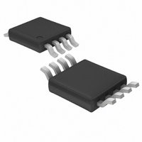
LT1567IMS8 Linear Technology, LT1567IMS8 Datasheet - Page 9

LT1567IMS8
Manufacturer Part Number
LT1567IMS8
Description
IC BLOCK BUILD FLTR LONOIS 8MSOP
Manufacturer
Linear Technology
Type
General Purposer
Datasheet
1.LT1567CMS8.pdf
(16 pages)
Specifications of LT1567IMS8
Applications
Filter
Mounting Type
Surface Mount
Package / Case
8-MSOP, Micro8™, 8-uMAX, 8-uSOP,
Filter Type
Universal
Order Filter (max)
2nd
Dual Supply Voltage (typ)
±3/±5V
Power Supply Requirement
Single/Dual
Operating Temperature (min)
-40C
Operating Temperature (max)
85C
Lead Free Status / RoHS Status
Contains lead / RoHS non-compliant
APPLICATIO S I FOR ATIO
The simple-to-use spreadsheet requires the user to de-
fine the desired corner (or center) frequency, the pass-
band gain and a capacitor value for a choice of second or
third order Chebyshev or Butterworth lowpass or second
order bandpass filters.
The spreadsheet outputs the required external standard
component values and provides a circuit diagram.
Signal Ground
Both operational amplifiers within the LT1567 are de-
signed for inverting operation (constant common mode
V
IN
R1
R2
C2
C1
U
0.1µF
R3
3
5
2
U
LT1567
Figure 2. 2nd Order Bandpass Filter and Gain Response for f
Gain = 10 (C1 = C2 = 1000pF, R2 = R3 = 1.05k, R1 = 105Ω)
–
+
150Ω
8
W
V
V
+
+
0.1µF
GAIN IS MEASURED TO EITHER OUTPUT ALONE.
IF OUTPUT USED DIFFERENTIALLY, V
–10
–15
–5
25
20
15
10
7pF
5
0
1
50k
6
600Ω
U
–
+
Gain vs Frequency
600Ω
4
V
FREQUENCY (Hz)
–
V
–
0.1µF
500k
input) and they share a single reference node on the chip.
Two pins permit access to this node: DC BIAS and
BYPASS. For a clean reference over a wide bandwidth, the
normal procedure is to connect DC BIAS to a DC potential
or ground and BYPASS to a decoupling capacitor that
returns to a ground plane.
Differential Output Feature
The multiple feedback filter section of Figure 1 inherently
includes two outputs of opposite signal polarity: a DC
inverting output from the OA (Pin 1) and a DC noninverting
OUT
7
+
– V
1567 F02a
OUT
V
V
1567 F02b
OUT
OUT
–
= 2× V
5M
–
+
IN
DESIGN EQUATIONS FOR f
f
MAXIMUM f
GN IS GAIN AT f
f
C1 ≤
CENTER
CENTER
C
= 500kHz,
√GN + 1
2500 • f
IS THE FILTER’S CENTER FREQUENCY
=
2 • π • R2 • C1
CENTER
√GN + 1
C
CENTER
R3 =
= 5MHz/GAIN
2π • C1 • f
= R3/R1, R2 = R3, C1 = C2
CENTER
–3dB BANDWIDTH =
√GN + 1
CENTER
≤ 1MHz
LT1567
f
√GN + 1
CENTER
1567fa
9


