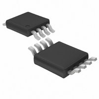
LTC1542IMS8#PBF Linear Technology, LTC1542IMS8#PBF Datasheet - Page 6

LTC1542IMS8#PBF
Manufacturer Part Number
LTC1542IMS8#PBF
Description
IC OPAMP/COMP/REF MICROPWR 8MSOP
Manufacturer
Linear Technology
Type
Amplifier, Comparator, Referencer
Datasheet
1.LTC1542CS8PBF.pdf
(12 pages)
Specifications of LTC1542IMS8#PBF
Applications
General Purpose
Mounting Type
Surface Mount
Package / Case
8-MSOP, Micro8™, 8-uMAX, 8-uSOP,
Lead Free Status / RoHS Status
Lead free / RoHS Compliant
Available stocks
Company
Part Number
Manufacturer
Quantity
Price
LTC1541/LTC1542
ELECTRICAL CHARACTERISTICS
temperature range, otherwise specifications are at T
SYMBOL
I
I
e
TYPICAL PERFOR A CE CHARACTERISTICS
6
Note 1: Absolute Maximum Ratings are those values beyond which the life
of the device may be impaired.
Note 2: Supply current is tested with COMPIN
LTC1541 and COMPIN
Note 3: Input offset voltage is defined as the center of the input referred
hysteresis, V
Note 4: Trip point is defined as the differential input voltage required to
make the comparator output change state. The difference between upper
and lower trip point is equal to the width of the input referred hysteresis,
V
Note 5: The input leakage current is measured for COMPIN
(LTC1541) and COMPIN
SOURCE
SINK
n
CM
10
9
8
7
6
5
4
3
2
1
0
= REF (LTC1541). V
2
Supply Current vs Supply Voltage
NONINVERTING
V
AMPIN
3
SS
CM
= GND
PARAMETER
Output Source Current
Output Sink Current
Input Noise Voltage
4
+
= REF (LTC1541). V
= V
SUPPLY VOLTAGE (V)
5
CC
/2
6
+
= 0V, COMPIN
+
CM
= COMPIN
7
= 1/2 V
8
9
CC
CM
–
W
10 11 12
(LTC1542).
= 0V (LTC1542).
–
1541/42 TPC01
= 1/2 V
= 100mV for LTC1542.
U
+
CC
= (REF – 100mV) for
(LTC1542).
CONDITIONS
f
O
= 0.1Hz to 10Hz
10
9
8
7
6
5
4
3
2
–50
+
Supply Current vs Temperature
A
at 0V
V
V
AMPIN
AMPIN
CC
SS
= 25°C. V
–25
= 5V
= GND
+
–
The
= AMPOUT
= 2.5V
0
TEMPERATURE (°C)
●
CC
25
denotes specifications which apply over the full operating
= 3V, V
Note 6: The θ
spreading metal. Using expanded metal area on all layers of a board
reduces this value.
Note 7: The LTC1541C/LTC1541I and LTC1542C/LTC1542I are
guaranteed functional over the operating temperature range of –40°C to
85°C.
Note 8: The LTC1541C and LTC1542C are guaranteed to meet specified
performance from 0°C to 70°C. The LTC1541C and LTC1542C are
designed, characterized and expected to meet performance from –40°C to
85°C, but are not tested or QA sampled at these temperatures. The
LTC1541I and LTC1542I are guaranteed to meet specified performance
from –40°C to 85°C.
50
SS
75
= 0V, unless otherwise noted.
1541/42 TPC02
100
JA
specified for the DD package is with minimal PCB heat
125
1.205
1.204
1.203
1.202
1.201
1.200
1.199
1.198
1.197
1.196
1.195
●
●
1
Reference Output Voltage vs
Load Current
V
V
CC
SS
= 5V
= GND
MIN
0.6
0.4
1.2
0.8
10
LOAD CURRENT (µA)
0.95
TYP
1.8
3
100
SINKING
CURRENT
SOURCING
CURRENT
MAX
1000
1541/42 TPC03
UNITS
15412fd
µV
10000
mA
mA
mA
mA
P-P


